
Method and apparatus for memory self testing

a memory and self-testing technology, applied in the field of data processing systems, can solve the problems of loss of test quality, difficulty in providing a generic memory self-test system, and inability to properly implement self-test algorithms such as a “bitline stress test” or a “checkerboard test” to achieve the effect of ensuring memory test accuracy and being easy to accommoda

Active Publication Date: 2006-09-07
ARM LTD
View PDF8 Cites 19 Cited by
  • Summary
  • Abstract
  • Description
  • Claims
  • Application Information

AI Technical Summary

Benefits of technology

The present invention provides an apparatus for processing data that includes a self-test controller and a programmable re-mapper. The self-test controller is operable in a self-test mode to generate a sequence of memory addresses for performing memory access operations in accordance with a memory test algorithm having a physical configuration. The programmable re-mapper is responsive to programmable mapping selection data to re-map the sequence of generated memory addresses in a programmable manner. This allows the self-test controller to test the intended memory cell physical access pattern regardless of the memory system under test. The programmable re-mapper can efficiently reassign addressing in the memory system to compensate for differences in implementation. The self-test instruction includes a sequence of generated memory addresses and mapping selection data, which can be programmed to target different memory cell physical access patterns for a given sequence of generated memory addresses. The invention is particularly well suited to use with integrated circuits.

Problems solved by technology

This presents a difficulty in provision of a generic memory self-test system, since BIST self-test algorithms target particular memory cell physical access patterns to expose particular memory defects.
Failure to address memory cells according to the intended physical access patterns may result in loss of test quality, since in this case the algorithms no longer address the intended particular physical memory cells (locations) in precise sequential steps.
Thus, self-test algorithms such as a “bitline stress test” or a “checkerboard test” would not be correctly implemented if the memory cell physical access pattern did not match the intended memory cell physical access pattern due to differences in mappings between memory address indices and physical locations (i.e. cells) of a memory array.

Method used


Image

  • Method and apparatus for memory self testing
  • Method and apparatus for memory self testing
  • Method and apparatus for memory self testing

Examples


Embodiment Construction

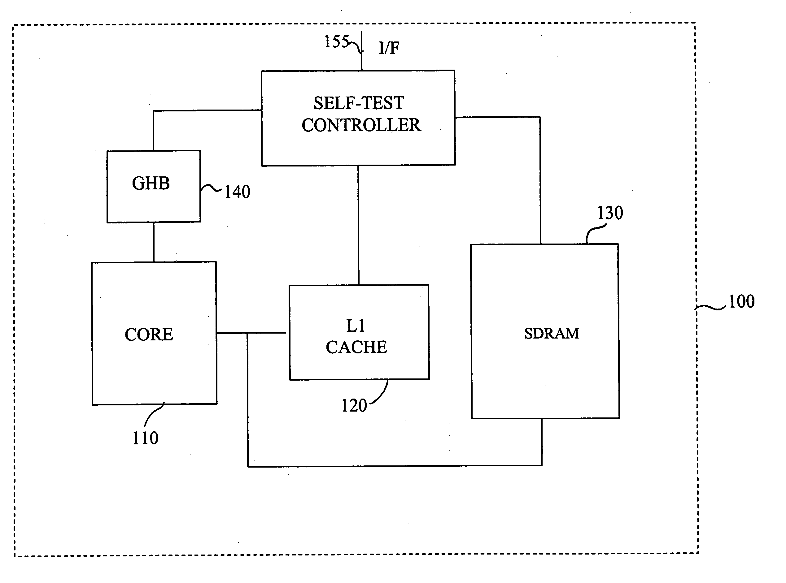
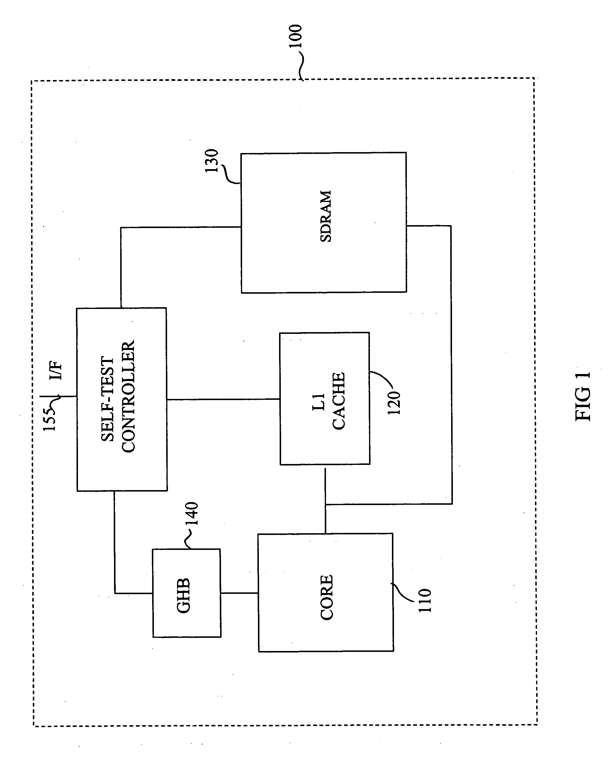
[0049]FIG. 1 schematically illustrates an integrated circuit 100 comprising a processor core 110, an L1 cache memory 120, an SDRAM 130, a global history buffer 140 and a self-test controller 150. A self-test interface 155 is provided to enable supply data to the self-test controller 150. It will be appreciated that the integrated circuit 100 will typically comprise many additional circuit elements which have not been illustrated in FIG. 1 for the sake of simplicity and clarity.

[0050] The processor core has direct access to the L1 cache 120, which is formed of static random access memory (SRAM) which enables high-speed memory access. The core 110 also has access to the global history buffer 140, which is used to store data associated with branch prediction, and access to the SDRAM 130, which is slower memory than the L1 cache 120 and is used to store less frequently accessed data. The self-test controller 150 is connected to each of the L1 cache 120, the SDRAM 130 and the global his...


PUM


Abstract

A memory self-test system is provided comprising a self-test controller operable in self-test mode to generate a sequence of generated memory addresses for performing memory access operations associated with the memory test algorithm having an associated memory cell physical access pattern. A programmable re-mapper is operable to re-map the sequence of generated memory addresses derived from the self-test instruction to a sequence of re-mapped memory addresses. The programmable re-mapper performs this re-mapping in response to programmable mapping selection data. The re-mapping of the generated memory addresses to re-mapped memory addresses ensures that the memory cell accesses performed during execution of the memory self-test are consistent with the associated memory cell physical access pattern regardless of the particular implementation of the memory array.

Description

BACKGROUND OF THE INVENTION [0001] 1. Field of the Invention [0002] This invention relates to the field of data processing systems. More particularly, this invention relates to the self-testing of memories within data processing systems to detect memory defects. [0003] 2. Description of the Prior Art [0004] It is known to provide data processing systems incorporating memories with self-testing mechanisms, sometimes termed built-in self-test (BIST), such that when memory circuits have been fabricated, a series of self-tests can be performed to determine whether there are any memory defects present in that data processing system, which would indicate that circuits should be rejected. [0005] As technology progresses there is a trend for memory sizes to increase in order to enable provision of more advanced applications. Accordingly, the defect density of these larger memories is becoming increasingly significant and the self-testing requirements more onerous. Furthermore, the memory mo...

Claims


Application Information

Patent Timeline
Patent Type & Authority Applications(United States)
IPC IPC(8): G11C29/00
CPCG11C29/18G11C2029/1806G11C2029/3602
Inventor SLOBODNIK, RICHARDFREDERICK, FRANK DAVID
Owner ARM LTD
Learn More