Image pickup device and camera with expanded dynamic range

a pickup device and dynamic range technology, applied in the field of image pickup devices and image pickup systems, can solve problems such as deteriorating image quality

Inactive Publication Date: 2006-09-21
CANON KK
View PDF46 Cites 105 Cited by
  • Summary
  • Abstract
  • Description
  • Claims
  • Application Information

AI Technical Summary

Problems solved by technology

However such prior technologies involve a drawback that the image-pickup device often generates noises thereby possibly deteriorating the image quality.

Method used


Image

  • Image pickup device and camera with expanded dynamic range
  • Image pickup device and camera with expanded dynamic range
  • Image pickup device and camera with expanded dynamic range

Examples


Embodiment Construction

[0018] In the following, a first embodiment of the present invention will be explained with reference to the accompanying drawings.

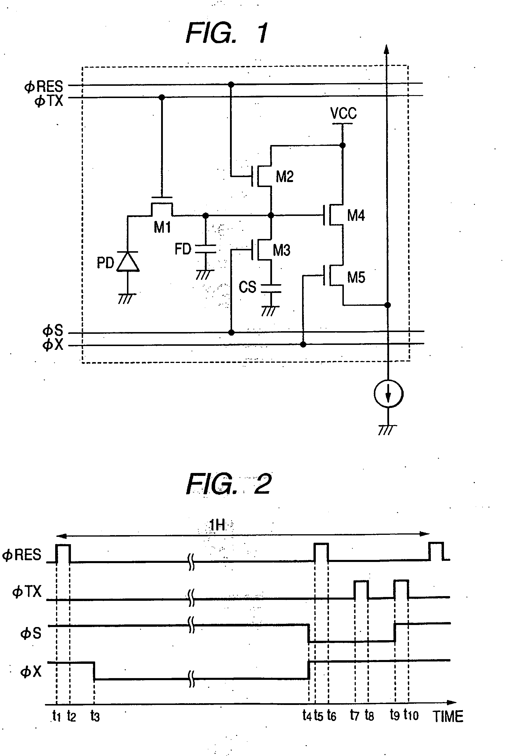
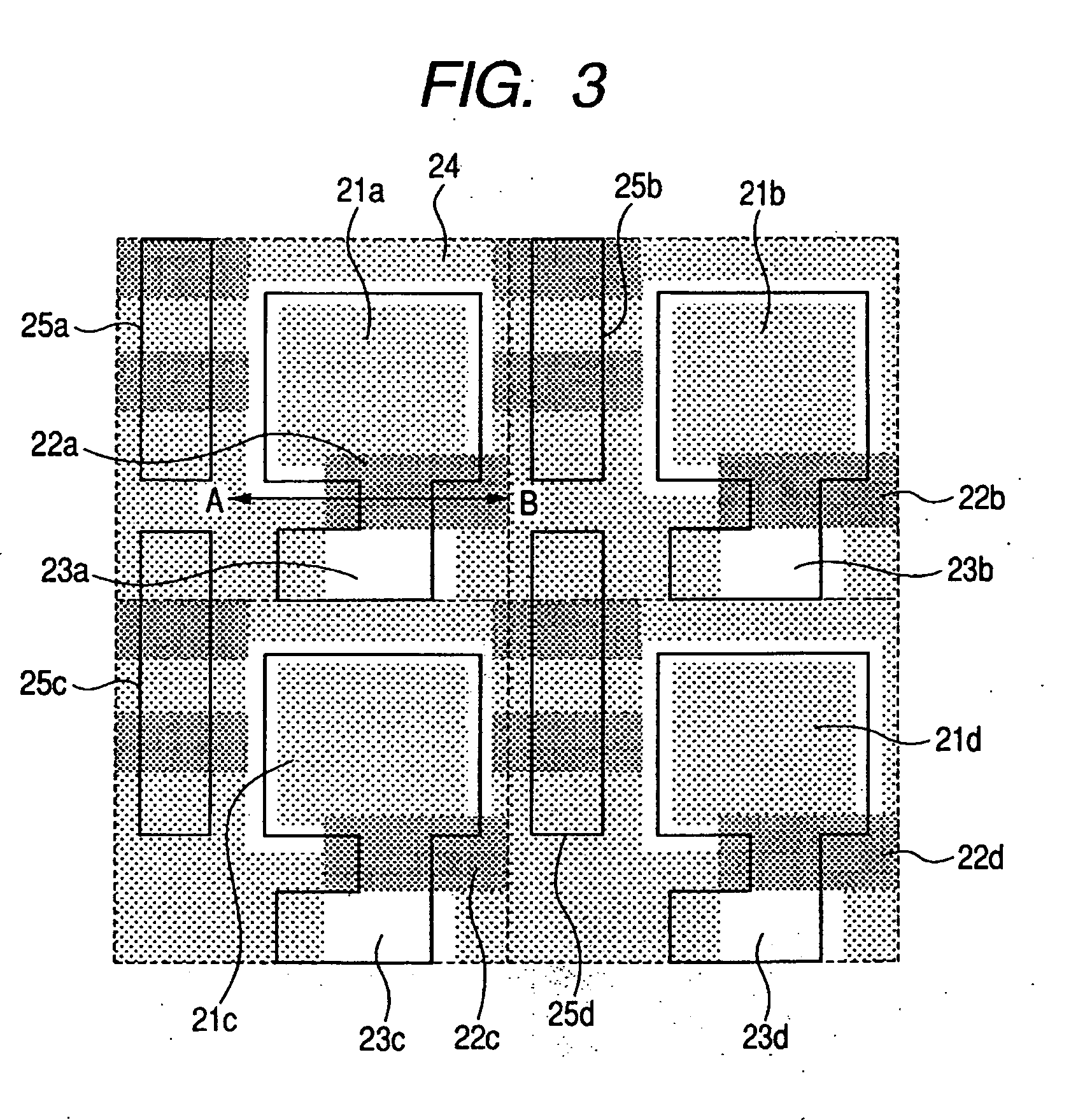
[0019]FIG. 1 illustrates a schematic structure of a pixel provided in the image pickup device of the present embodiment FIG., is a schematic plan view showing a layout of four pixels shown in FIG. 1, and FIG. 4A is a schematic cross sectional view along a line A-B.

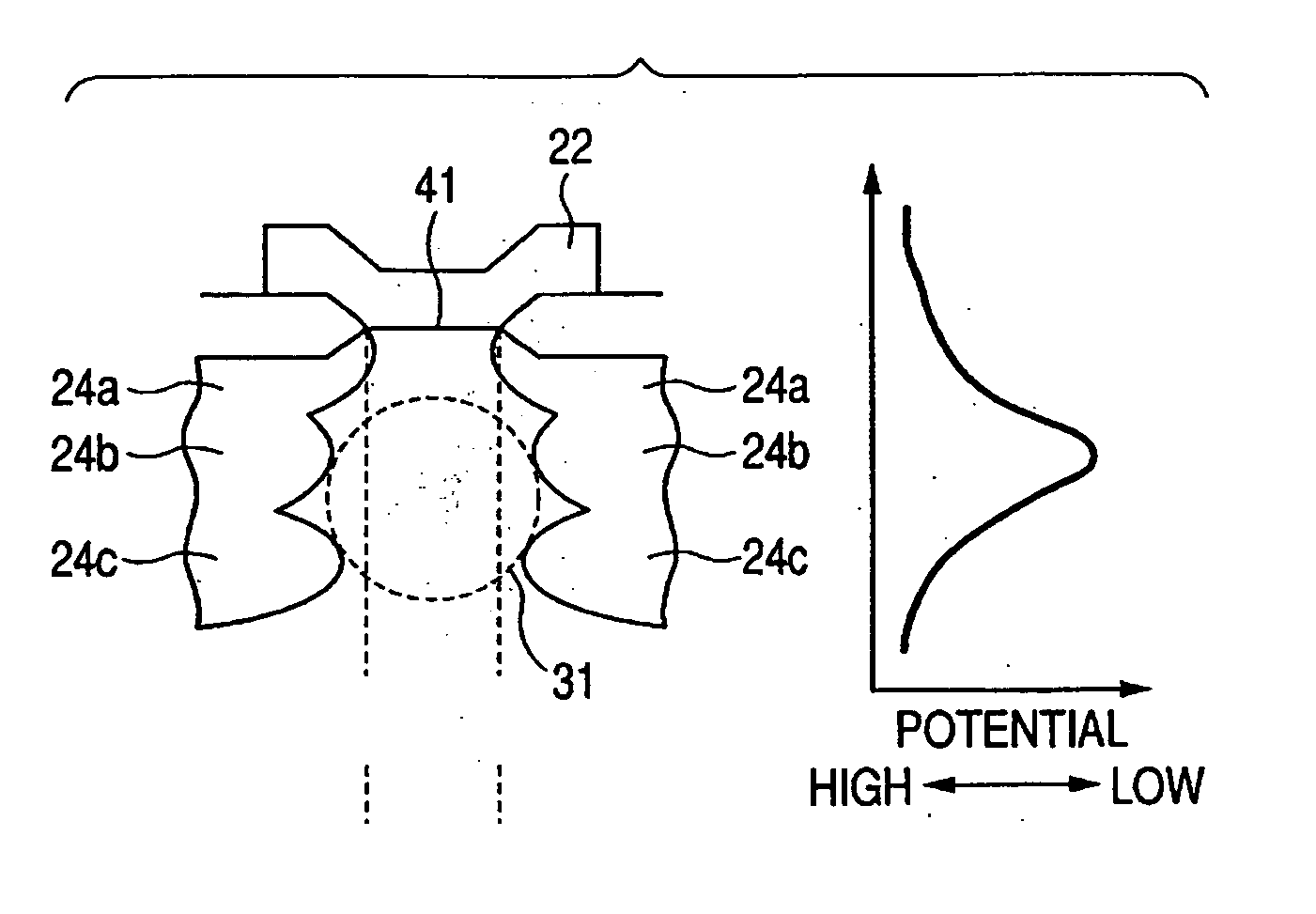
[0020] Also in contrast to the present embodiment, there is known a method of controlling (elevating) a gate potential of the transfer transistor for example at about 0 V, which carriers are accumulated in the photodiode constituting the photoelectric converting portion. In this method, the transfer transistor assumes an incompletely turned off state, whereby a part of the carriers overflowing from the photodiode flows into the floating diffusion region. Such carriers overflowing from the photodiode is used, together with the carriers accumulated in the photodiode, as a pixel signal to achiev...


PUM


Abstract

The image pickup device of the invention has a path deeper in a semiconductor substrate, than a region wherein a channel is formed, upon turning on a first MOS transistor, under a gate thereof. The path is arranged by forming a P-type layer for forming a potential barrier, within a P-type well excluding a region below the gate of the first MOS transistor. Thus, even when the first transfer MOS transistor is securely turned off at accumulation, carriers overflowing from a photodiode can flow into the path, thereby enabling to accumulate the carriers, overflowing from the photodiode, in a carrier accumulation region. Such structure allows to suppress a dark current generation from an interface of a gate oxide film of the first transfer MOS transistor, and also to expand the dynamic range of the image pickup device by the carriers overflowing from the photodiode and flowing through the path into the carrier accumulation region.

Description

BACKGROUND OF THE INVENTION: [0001] 1. Field of the Invention [0002] The present invention relates to an image pickup device and an image pickup system, and more particularly those adapted for employing a CMOS area sensor. [0003] 2. Related Background Art [0004] Recently, a CMOS area sensor formed by pixels, each including a photodiode and a MOS transistor, is being employed as an image, pickup device. The CMOS sensor has advantages, in comparison with a CCD area sensor, of a lower electric power consumption, a lower driving electric power and a possible high-speed operation. The demand for such CMOS area sensor is anticipated to grow hereafter. [0005] The CMOS sensor is constituted of pixels, each formed for example by a photodiode, a floating diffusion region, a transfer transistor for transferring carriers from the photodiode to the floating diffusion region, and a reset transistor for resetting the floating diffusion region to a predetermined potential. A plurality of such pixel...

Claims


Application Information

Patent Timeline
Patent Type & Authority Applications(United States)
IPC IPC(8): H01L31/113H01L27/146H04N5/335H04N5/355H04N5/361H04N5/369H04N5/374H04N5/376
CPCH01L27/14603H01L27/14609H01L27/14625H01L27/14643H01L27/14656H04N5/361H04N25/63
Inventor ITANO, TETSUYAKOIZUMI, TORUKIKUCHI, SHINOKITA, AKIRAOGURA, MASANORI
Owner CANON KK
Why Eureka
Try Eureka