Sidewall gate thin-film transistor

a thin-film transistor and sidewall gate technology, applied in the field of integrated circuit (ic) fabrication, can solve the problems of undesired rapid diffusion and dissipation of heat in laser irradiation, affecting the speed at which a circuit made by such device-blocks can operate, and the size of tfts formed in liquid crystal display (lcd) processes is limited, so as to improve the active channel crystallization, eliminate parasitic capacitive coupling, and the fabrication process process

Inactive Publication Date: 2006-11-02
SHARP LAB OF AMERICA INC
View PDF5 Cites 12 Cited by
  • Summary
  • Abstract
  • Description
  • Claims
  • Application Information

AI Technical Summary

Benefits of technology

[0011] The present invention describes a modified V-TFT architecture and the associated fabrication flow, which uses a SiO2 step structure to form the V-TFT. The device architecture is suitable for improved active channel crystallization, eliminates the parasitic capacitive coupling between V-T

Problems solved by technology

The size of TFTs formed in liquid crystal display (LCD) processes is limited by the resolution of large panel photolithography tools.
This overlap introduces a parasitic capacitance, which affects (decreases) the speed at which a circuit made by such device-blocks can operate.
An additional issue affecting

Method used


Image

  • Sidewall gate thin-film transistor
  • Sidewall gate thin-film transistor
  • Sidewall gate thin-film transistor

Examples


Embodiment Construction

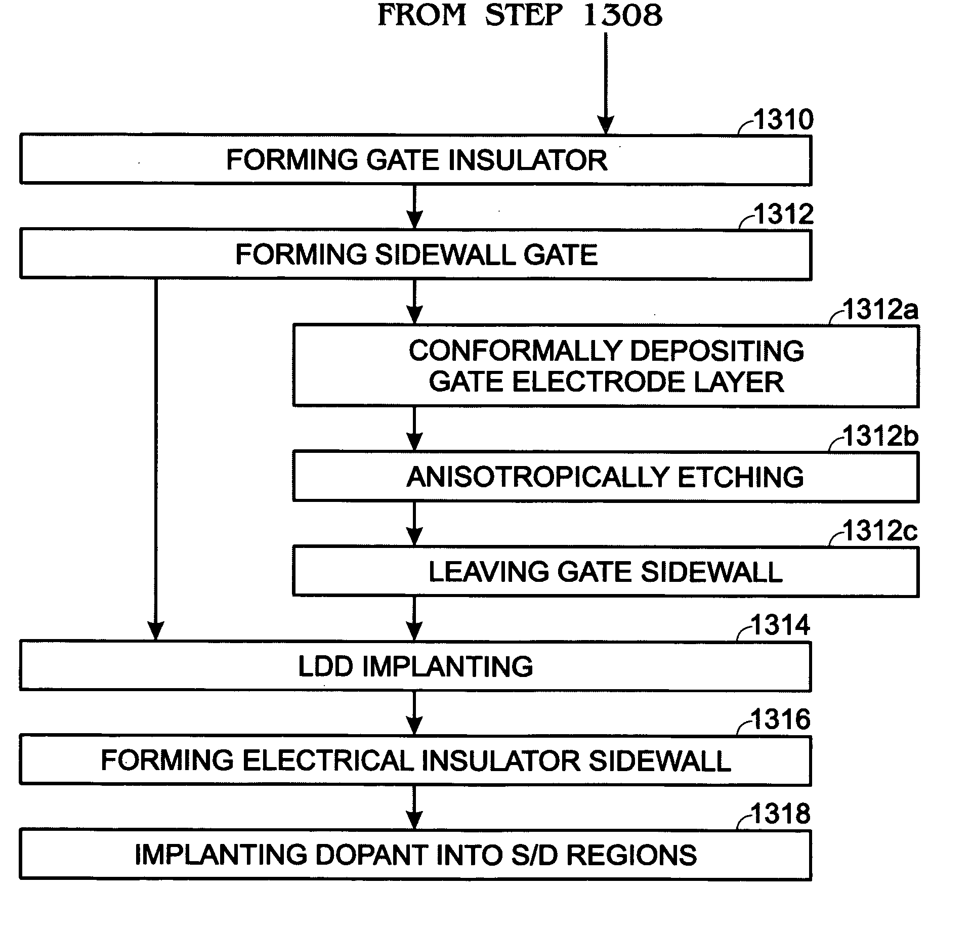
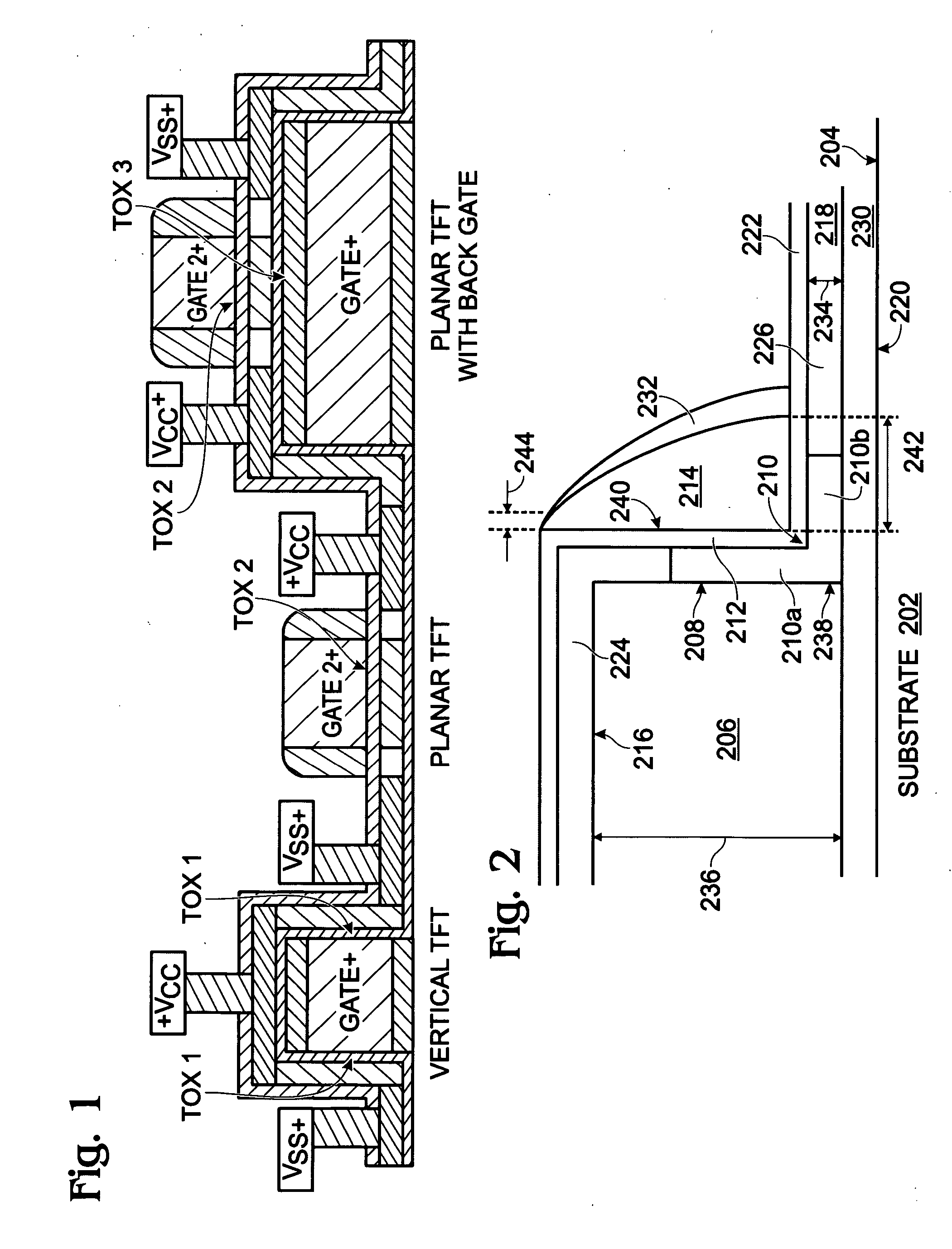
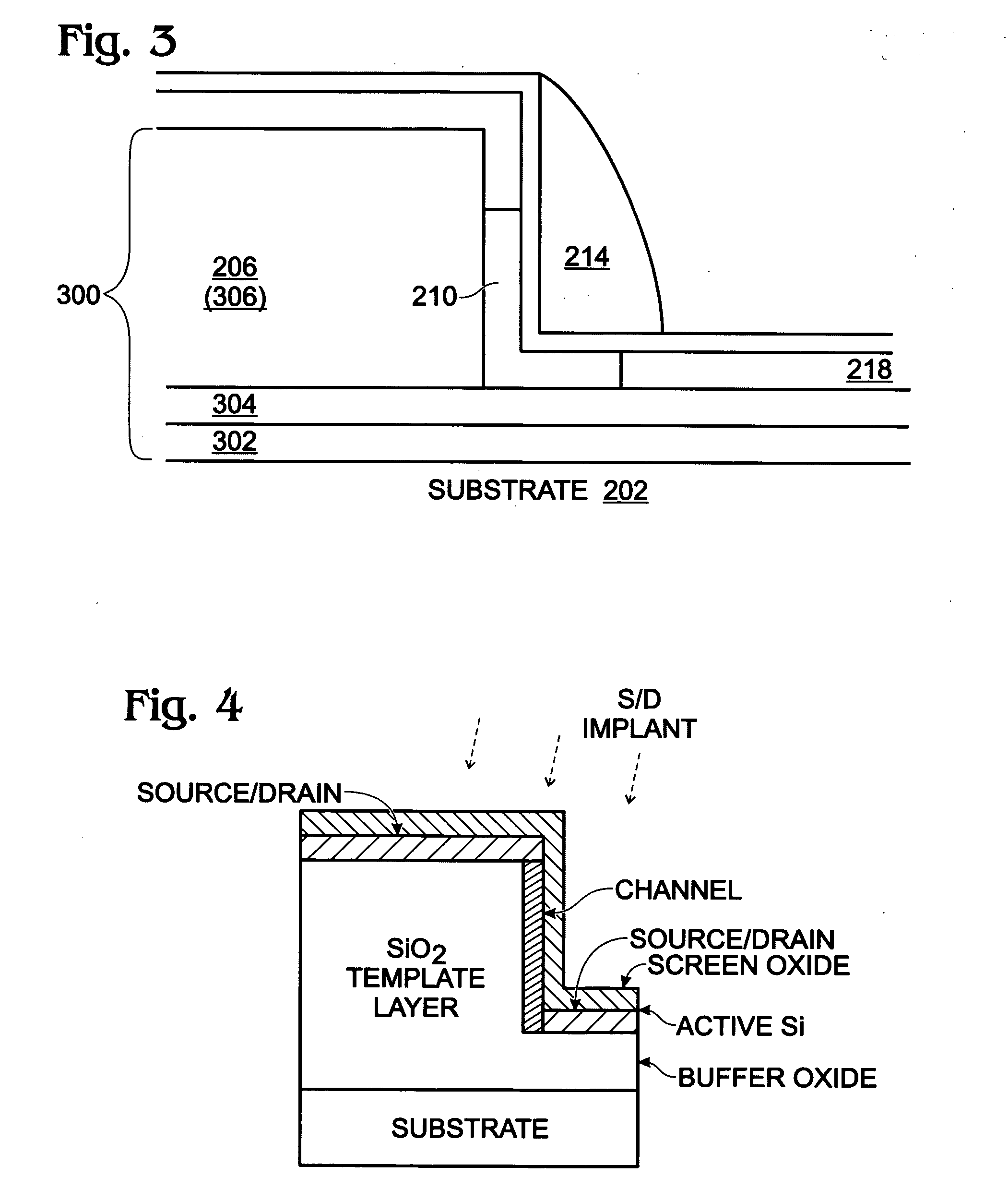
[0030]FIG. 2 is a partial cross-sectional view of a thin-film transistor (TFT) with a sidewall gate. The sidewall gate TFT 200 comprises a substrate 202 with a surface 204. A surface-normal feature 206, normal with respect to the substrate surface 204, has a sidewall 208 made from an electrical insulator. For example, the insulator may be silicon oxide or a silicon nitride material. Although the surface-normal feature is depicted here as a step, in other variations (not shown) the surface-normal feature can be a via, cavity, pillar, or the like. Further, although the feature 206 is shown as orthogonal to the substrate surface 204, in other aspects (not shown), the feature 206 may be formed at an angle with respect to the surface, as might be realistically expected using an etching process, which typically removes more from the top of a feature than the foot of a feature. Further, the sidewall may have a bowed or tapered shape. In fact, the surface normal feature is not limited to an...


PUM


Abstract

A sidewall gate thin-film transistor (TFT) and associated fabrication method are provided. The method provides a substrate with a surface and forms a surface-normal feature. The surface-normal feature is normal with respect to the substrate surface, with a sidewall made from an electrical insulator. An active silicon (Si) layer is formed overlying the surface-normal feature, with a channel overlying the surface-normal feature sidewall. A gate insulator overlies the channel, and a sidewall gate overlies the gate insulator. More specifically, the gate insulator is formed from conformally depositing an electrical insulator layer overlying the active Si layer. The gate electrode layer is conformally deposited overlying the gate insulator layer and anisotropically etched, leaving a gate electrode sidewall adjacent to the gate insulator layer overlying the channel.

Description

RELATED APPLICATIONS [0001] This application is a continuation-in-part of a pending patent application entitled, MULTI-PLANAR LAYOUT VERTICAL THIN-FILM TRANSISTOR INVERTER, Schuele et al., Ser. No. 10 / 862,761, filed Jun. 7, 2004, Attorney Docket No. SLA0875, which is a continuation-in-part of an issued patent application entitled, VERTICAL THIN FILM TRANSISTOR, invented by Schuele et al., U.S. Pat. No. 6,995,053, filed Apr. 23, 2004, Attorney Docket No. SLA0874. [0002] This application is a continuation-in-part of a pending patent application entitled, DUAL-GATE THIN-FILM TRANSISTOR, invented by Schuele et al., Ser. No. 10 / 953,913, filed Sep. 28, 2004, Attorney Docket No. SLA0909.BACKGROUND OF THE INVENTION [0003] 1. Field of the Invention [0004] This invention generally relates to integrated circuit (IC) fabrication and, more particularly, to a sidewall gate thin-film transistor (TFT) and associated fabrication process. [0005] 2. Description of the Related Art [0006] The size of TF...

Claims


Application Information

Patent Timeline
IPC IPC(8): H01L21/84H01L21/00
CPCH01L27/1214H01L29/78642H01L29/6675H01L27/1251
Inventor VOUTSAS, APOSTOLOS T.SCHUELE, PAUL J.
Owner SHARP LAB OF AMERICA INC
Why Eureka
Try Eureka