Local sonos-type structure having two-piece gate and self-aligned ono and method for manufacturing the same

Inactive Publication Date: 2004-09-23
SAMSUNG ELECTRONICS CO LTD
View PDF4 Cites 81 Cited by
  • Summary
  • Abstract
  • Description
  • Claims
  • Application Information

AI Technical Summary

Problems solved by technology

Because of the high threshold voltage Vth and the high program current, it is difficult to embed the stack SONOS in system-on-a-chip (SoC) products which demand low power consumption.
In addition, in the stacked SONOS-type cell 10, electrons trapped in th

Method used


Image

  • Local sonos-type structure having two-piece gate and self-aligned ono and method for manufacturing the same
  • Local sonos-type structure having two-piece gate and self-aligned ono and method for manufacturing the same
  • Local sonos-type structure having two-piece gate and self-aligned ono and method for manufacturing the same

Examples


Embodiment Construction

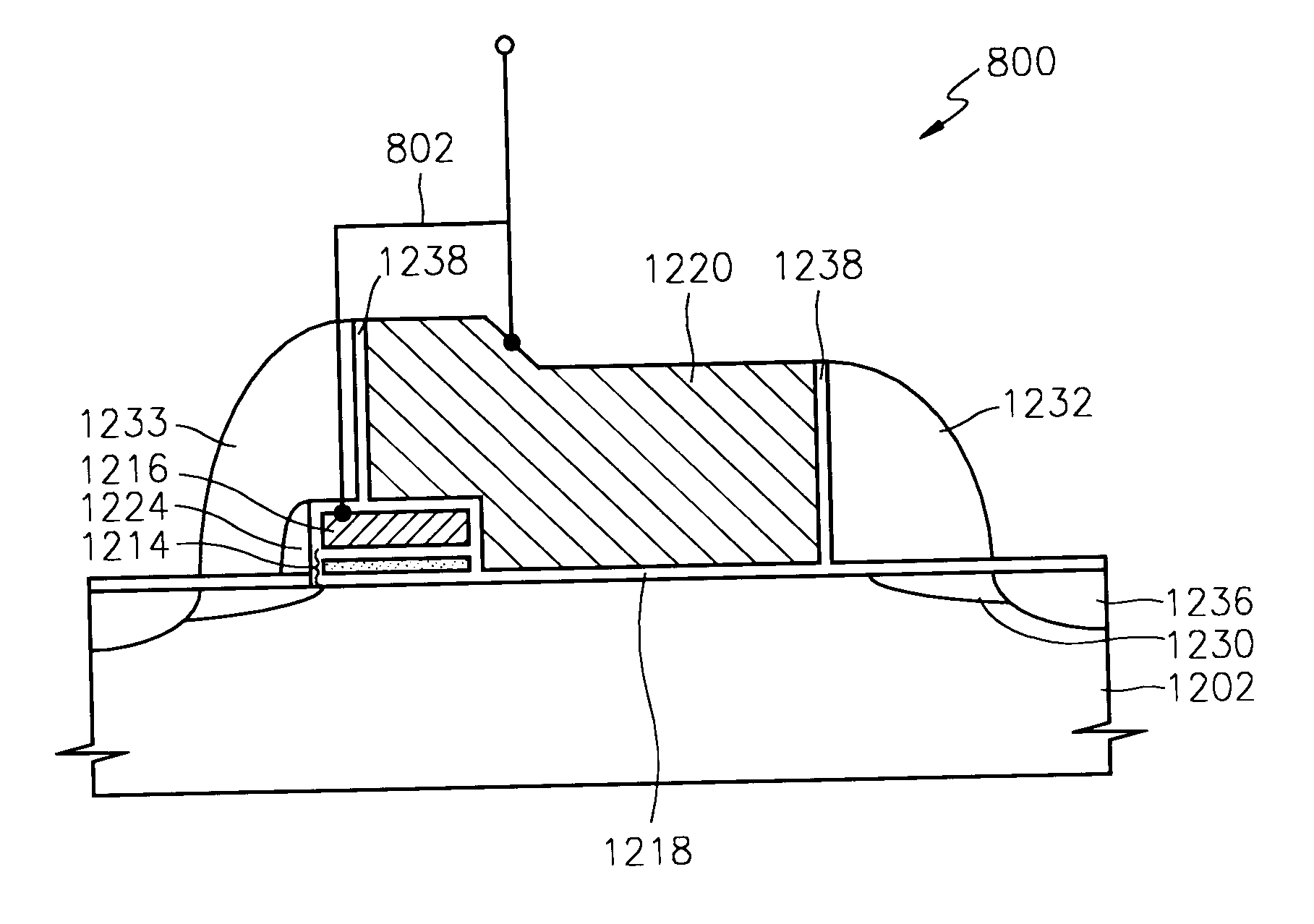
[0037] An embodiment of the invention is the recognition that variation in the overlap length, L (between a gate electrode and an ONO-type structure), can be negated as a problem if the gate electrode is formed as a two-piece structure, where the ONO-type structure is self-aligned with the first piece of the gate electrode. In other words, this embodiment is a recognition that alignment tolerance of the upper or second piece of the two-part gate electrode substantially does not induce variation in the threshold voltage Vth if the ONO-type structure is self-aligned with the lower or first electrode of the two-piece gate electrode.

[0038] FIG. 6 is a cross-section of a local SONOS-type structure 600 having a two-piece gate configuration according to an embodiment of the invention. The structure 600 can be used, e.g., in nonvolatile semiconductor memory devices such as are found in mobile telecommunication systems, memory cards, compact processor-based electronics, etc.

[0039] The struct...


PUM


Abstract

A local SONOS structure having a two-piece gate and a self-aligned ONO structure includes: a substrate; an ONO structure on the substrate; a first gate layer on and aligned with the ONO structure; a gate insulator on the substrate aside the ONO structure; and a second gate layer on the first gate layer and on the gate insulator. The first and second gate layers are electrically connected together. Together, the ONO structure and first and second gate layers define at least a 1-bit local SONOS structure. A corresponding method of manufacture includes: providing a substrate; forming an ONO structure on the substrate; forming a first gate layer on and aligned with the ONO structure; forming a gate insulator on the substrate aside the ONO structure; forming a second gate layer on the first gate layer and on the gate insulator; and electrically connecting the first and second gate layers.

Description

DESCRIPTION OF THE BACKGROUND ART[0001] In general, semiconductor memory devices for storing data are divided into volatile memory devices, which are likely to lose their data when the power supply is interrupted, and nonvolatile memory devices, which can retain their data even when the power supply is interrupted. Compared to other nonvolatile memory technologies, e.g., disk drives, nonvolatile semiconductor memories are relatively small. Accordingly, nonvolatile memory devices have been widely employed in mobile telecommunications systems, memory cards, etc.[0002] Recently, nonvolatile memory devices having silicon-oxide-nitride-o-xide-silicon (SONOS) structures, e.g., SONOS-type nonvolatile memory devices, have been proposed. The SONOS-type nonvolatile memory devices have thin cells which are simple to manufacture and can be easily incorporated, e.g., into a peripheral region and / or a logic region of an integrated circuit.[0003] A SONOS-type nonvolatile semiconductor memory devic...

Claims


Application Information

Patent Timeline
IPC IPC(8): H01L21/8246H01L21/8247H01L27/115H01L29/423H01L29/788H01L29/792
CPCH01L29/792Y10S438/954H01L29/7923H10B69/00
Inventor BAE, GEUM-JONGLEE, NAE-INKIM, SANG SUKIM, KI CHULKIM, JIN-HEECHO, IN-WOOKKIM, SUNG-HOKOH, KWANG-WOOK
Owner SAMSUNG ELECTRONICS CO LTD
Why Eureka
Try Eureka