This helps you quickly interpret patents by identifying the three key elements:
Problems solved by technology
Method used
Benefits of technology
Problems solved by technology
However, various problems have recently arisen due to the limitations of material properties.
To describe one of the foregoing problems, there is a problem that it is difficult to control the threshold voltage of a MISFET.
However, if the foregoing method is employed, carrier mobility is reduced; for this reason, the on / off characteristic of the MISFET is degraded.
However, the threshold voltage control for the MISFET is not achieved according to the method of controlling the impurity concentration in channel only.
However, if quite different gate electrode materials are used, the manufacturing method becomes complicated, and the cost increases.
However, the foregoing methods do not meet the requirements described above.
However, heat resistance is low, and the work function irregularly varies by heat treatment of about 500° C. or more at least.
Thus, the correlation is thermally unstable.
As a result, there is a problem that the on / off characteristic of the MISFET is degraded.
However, the variable range of the work function is insufficient to obtain a sufficiently low threshold voltage in a bulk MISFET device, which is not the fully-depleted MISFET device.
Method used
Image
Click on the blue label to locate the original text in one second.
Reading with bidirectional positioning of images and text.
Examples
first embodiment
[0059] (First Embodiment)
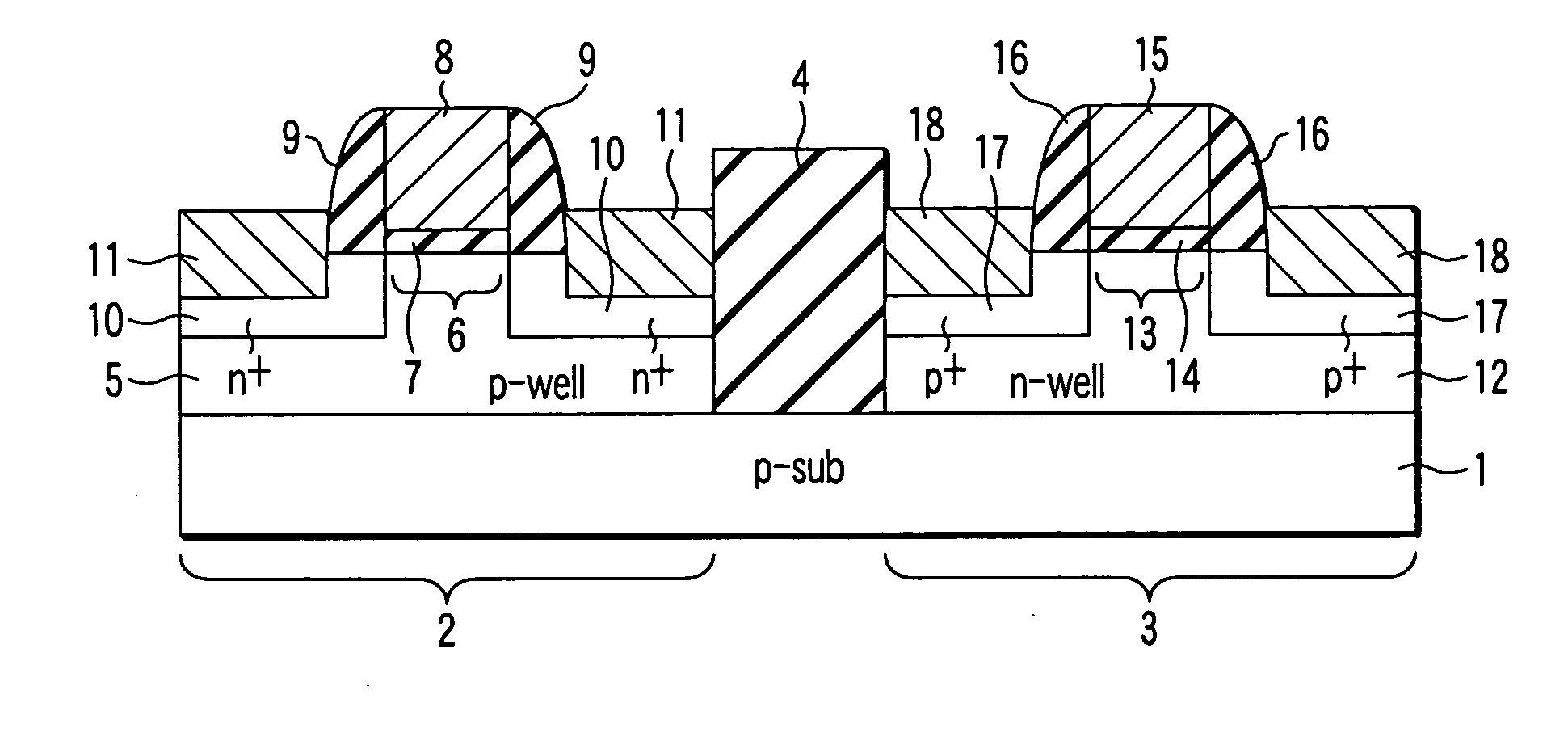
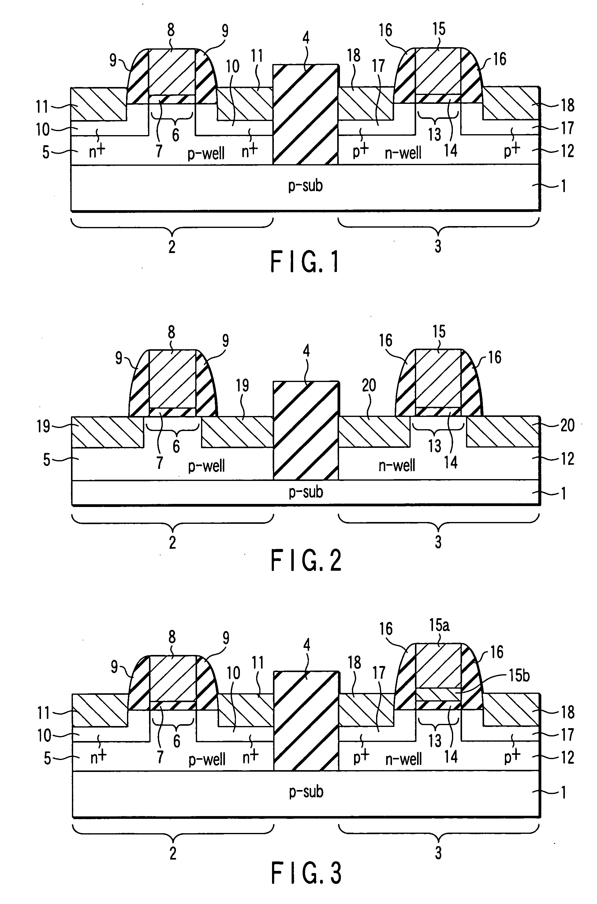
[0060] A CMISFET according to the first embodiment will be described below with reference to FIG. 1. As shown in FIG. 1, an n-MISFET 2 and a p-MISFET 3 are formed on a p-type silicon substrate 1 in a state of being isolated from an isolation region 4.
[0061] First, the n-MISFET 2 will be explained below. A p-well 5 (p-type impurity region) is formed on the p-type silicon substrate 1. The center of the upper portion of the p-well 5 is formed with an n-channel region 6. The n-channel region calls a region formed with an n-channel when gate voltage is applied. A first gate insulator 7 is formed on the n-channel region 6, and a first gate electrode 8 is formed on the first gate insulator 7. The first gate electrode 8 is interposed between first gate sidewall insulators 9. A pair of n-type source / drain regions 10 (n-type highly-doped impurity region) is formed on the opposite position via the n-channel region 6 on the p-well 5. The upper portion of the n-type sou...
second embodiment
[0089] (Second Embodiment)
[0090] A CMISFET according to the second embodiment will be described below in the point different from the first embodiment. The CMISFET of the second embodiment is based on the same technical concept as the CMiSFET of the first embodiment. However, the second embodiment differs from the first embodiment in that C is doped to the gate electrode. Therefore, the CMISFET of the second embodiment has the same cross-sectional structure as the first embodiment. Thus, the CMISFET of the second embodiment will be described below with reference to FIG. 1.
[0091] A compound M(SiGeC) of metal element M and group IV semiconductor element SiGeC is used as the material of the first and second gate electrodes 8 and 15. In the composition, group IV semiconductor elements, that is, Ge and C are solid-soluble in at least one gate electrode. More specifically, the material of the first gate electrode 8 is M(Si1−a−b GeaCb) (0≦a≦1, 0≦b≦0.02, 0≦a+b≦1). The material of the secon...
third embodiment
[0098] (Third Embodiment)
[0099] A CMISFET according to the third embodiment will be described in the point different from the first embodiment. The CMISFET according to the third embodiment has features given below. More specifically, several metal elements are used as M of the gate electrode material M(SiGe) of the CMISFET according to the first embodiment, and the M(SiGe) has the same crystal structure. Therefore, the CMISFET of the third embodiment has the same cross-sectional structure as the first embodiment. Thus, the CMISFET of the third embodiment will be described below with reference to FIG. 1.
[0100] A compound M(SiGe) of metal element M and group IV semiconductor element is used as the material of the first and second gate electrodes 8 and 15, like the first embodiment. In this case, M is two or more metal elements selected from Ni, Pd and Pt, or Ti and Zr.
[0101] The following is an explanation about Ni, Pd and Pt. According to the third embodiment, the foregoing mixed ...
PUM
Abstract
A semiconductor device comprises n-type and p-type semiconductor devices formed on the substrate, the n-type device including an n-channel region formed on the substrate, n-type source and drain regions formed opposite to each other interposing the n-channel region therebetween, a first gate insulator formed on the n-channel region, and a first gate electrode formed on the first gate insulator and including a compound of a metal M and a first group-IV elements Si1−a Gea (0≦a≦1), the p-type device including a p-channel region formed on the substrate, p-type source and drain regions formed opposite to each other interposing the p-channel region therebetween, a second gate insulator formed on the p-channel region, and a second gate electrode formed on the second gate insulator, and including a compound of the metal M and a second group-IV element Si1−c Gec (0≦c≦1, a≠c).
Description
CROSS-REFERENCE TO RELATED APPLICATIONS [0001] This application is based upon and claims the benefit of priority from prior Japanese Patent Application No. 2003-407658, filed Dec. 5, 2003, the entire contents of which are incorporated herein by reference. BACKGROUND OF THE INVENTION [0002] 1. Field of the Invention [0003] The present invention relates to a semiconductor device including a field effecttransistor. [0004] 2. Description of the Related Art [0005] In order to achieve high functionality of integrated circuits, elements forming the integrated circuits, that is, MISFETs (Metal-Insulator-SemiconductorField Effect Transistors) and CMISFETs (Complementary-MISFETs) need to have high performance. The MISFET is a metal-insulator-semiconductor field effecttransistor and the CMISFET is a complementary metal-insulator-semiconductor field effecttransistor. Basically, high performance of these elements has been achieved according to scaling law. However, various problems have rece...
Claims
Application Information
Patent Timeline
Application Date:The date an application was filed.
Publication Date:The date a patent or application was officially published.
First Publication Date:The earliest publication date of a patent with the same application number.
Issue Date:Publication date of the patent grant document.
PCT Entry Date:The Entry date of PCT National Phase.
Estimated Expiry Date:The statutory expiry date of a patent right according to the Patent Law, and it is the longest term of protection that the patent right can achieve without the termination of the patent right due to other reasons(Term extension factor has been taken into account ).
Invalid Date:Actual expiry date is based on effective date or publication date of legal transaction data of invalid patent.

