Method of making semiconductor device and semiconductor device

a semiconductor device and semiconductor technology, applied in semiconductor devices, semiconductor/solid-state device details, electrical devices, etc., can solve problems such as physical limits, difficulty in achieving higher performance, and in maintaining proper operation

Inactive Publication Date: 2008-07-31
KK TOSHIBA
View PDF12 Cites 81 Cited by
  • Summary
  • Abstract
  • Description
  • Claims
  • Application Information

AI Technical Summary

Benefits of technology

[0017]In accordance with the invention, it is possible to provide the semiconductor device which includes a MISFET having a strained channel ...

Problems solved by technology

In recent years, however, it is likely that this approach has almost reached physical limits and thus is faced with difficulties not only in achieving higher performances of circuit elements by miniaturization but also in retaining proper operations of such downscaled circuit elements per se.
One of such physical limits is a problem of parasitic resistance of source/drain (S/D) region.
Reducing the Schottky barrier height and tunnel distance leads to a decrease in interface resistance.
Obviously t...

Method used


Image

  • Method of making semiconductor device and semiconductor device
  • Method of making semiconductor device and semiconductor device
  • Method of making semiconductor device and semiconductor device

Examples


embodiment 1

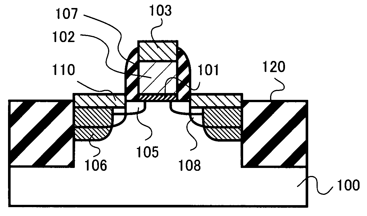
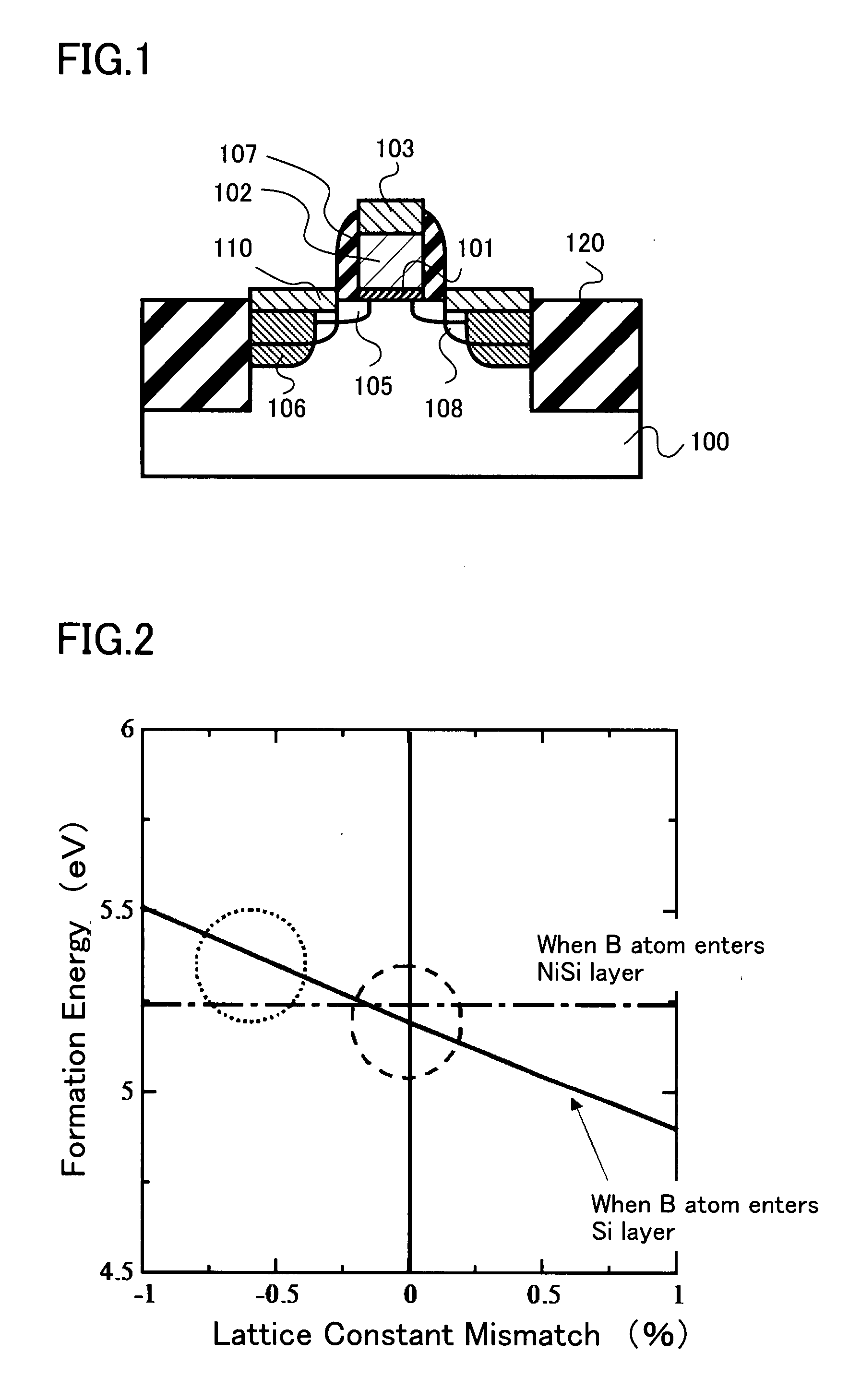
[0049]A fabrication process of the PMISFET shown in FIG. 1 will be described with reference to FIGS. 4 to 11 below. Firstly as shown in FIG. 4, an n-type silicon (Si) substrate 100 is prepared, which has its top surface corresponding to a (100) crystal plane and which is doped with phosphorus (P) to a concentration of about 1015 atoms / cm3. Then, form in the substrate surface a film of silicon oxide (SiOx) which provides shallow trench isolation (STI) regions 120 for electrical separation of circuit elements. Thereafter, form thereon a gate insulating film 101 to an equivalent oxide thickness (EOT) of about 1 nm. Next, deposit on this film a polycrystalline silicon or “poly-Si” film to a thickness of about 100 to 150 nm, by low-pressure chemical vapor deposition (LPCVD) techniques.

[0050]Then, as shown in FIG. 5, use lithography and etch techniques, such as reactive ion etching (RIE), to pattern the gate insulator film 101 and gate electrode 102 so that the resulting gate length is ...

embodiment 2

[0069]A semiconductor device fabrication method also embodying the invention is shown in FIGS. 13 to 16. This method is similar in principles to that shown in FIGS. 4-11, with the heavily B-doped active layers of PMISFET being formed by an epitaxial growth technique rather than the ion implantation in a way as will be described below.

[0070]After having performed the process steps shown in FIGS. 4-8, selective epitaxial growth is performed with mixture of a raw material gas of boron (B) to thereby form a couple of heavily B-doped thin diffusion layers 108 of p+-type conductivity on the exposed surfaces of recesses in Si substrate 100 as shown in FIG. 13. The p+-type diffusions 108 are 5×10²⁰ or more in impurity concentration.

[0071]Then, as shown in FIG. 14, after having formed the p+-type thin diffusion layers 108, change the raw gas to permit SixGe1-x layers 106 (where 0≦x108 to fill the recesses in Si substrate 100. At this time the underlying p+-type diffusions 108 are applied a c...

embodiment 3

[0075]A semiconductor device fabrication method in accordance with still another embodiment of the invention is shown in FIGS. 17 to 21. This method is similar to that stated supra with reference to FIGS. 13-16, except that B ion is heavily doped into an entirety of SiGe layer during the epitaxial growth of SiGe layer of PMISFET and that no extension layers are formed.

[0076]After having performed the process steps shown in FIGS. 4-5, deposit by LPCVD a silicon nitride (SiN) film to a thickness of about 8 nm. Then, perform etch-back by RIE techniques, thereby forcing the SiN film to selectively reside on the opposite sidewall faces of poly-Si gate electrode 102 as shown in FIG. 17. Thus the “first” gate sidewall insulator films 104 are formed.

[0077]Next, as shown in FIG. 18, with the poly-Si gate electrode 102 and first sidewall insulators 104 as a mask, selectively etch the exposed surface portions of Si substrate 100 to thereby dig it to a depth of about 30 nm. Thus, recess portion...


PUM


Abstract

A metal insulator semiconductor field effect transistor (MISFET) having a strained channel region is disclosed. Also disclosed is a method of fabricating a semiconductor device having a low-resistance junction interface. This fabrication method includes the step of forming a gate electrode above a silicon substrate with a gate insulator film being sandwiched therebetween. Then, form a pair of heavily-doped p (p+) type diffusion layers in or on the substrate surface at both sides of the gate electrode to a concentration of 5×10¹⁹ atoms/cm3 or more and yet less than or equal to 1×10²¹ atoms/cm3. Next, silicidize the p+-type layers by reaction with a metal in the state that each layer is applied a compressive strain.

Description

CROSS-REFERENCE TO RELATED APPLICATION[0001]This application is based upon and claims the benefit of priority from the prior Japanese Patent Application No. 2007-015990, filed Jan. 26, 2007, the entire content of which is incorporated herein by reference.FIELD OF THE INVENTION[0002]The present invention relates to a semiconductor device fabrication method for improvement of the source / drain regions of metal insulator semiconductor field effect transistors (MISFETs). This invention also relates to semiconductor devices as fabricated by the method.BACKGROUND OF THE INVENTION[0003]Silicon-based ultralarge-scale integrated (ULSI) circuitry is one of infra-technologies that support advanced information society in near future. For further functional improvement of ULSI circuits, it is inevitable to enhance performances of MISFETs, which are major elements of ULSI circuit devices. Traditionally the performance enhancement of on-chip circuit elements has fundamentally relied upon miniaturiz...

Claims


Application Information

Patent Timeline
IPC IPC(8): H01L29/78H01L21/336H01L23/48
CPCH01L21/26513H01L29/785H01L21/823807H01L21/823814H01L29/165H01L29/47H01L29/66507H01L29/6653H01L29/6659H01L29/66636H01L29/66643H01L29/66795H01L29/7833H01L29/7848H01L21/324
Inventor YAMAUCHI, TAKASHIKINOSHITA, ATSUHIROTSUCHIYA, YOSHINORIKOGA, JUNJI
Owner KK TOSHIBA
Why Eureka
Try Eureka