A semiconductor structure with multiple active regions and its preparation method

A technology of semiconductor and active area, applied in the field of multi-active area semiconductor structure and its preparation, to achieve the effects of reducing spacing, increasing tunneling probability, and reducing resistance

Active Publication Date: 2022-04-22
SUZHOU EVERBRIGHT PHOTONICS CO LTD +1
View PDF0 Cites 0 Cited by
  • Summary
  • Abstract
  • Description
  • Claims
  • Application Information

AI Technical Summary

Problems solved by technology

[0004] Therefore, the technical problem to be solved by the present invention is to overcome the problem of effectively improving luminous efficiency and reducing optical field crosstalk in the prior art, so as to provide a semiconductor structure with multiple active regions and its preparation method

Method used


Image

  • A semiconductor structure with multiple active regions and its preparation method
  • A semiconductor structure with multiple active regions and its preparation method
  • A semiconductor structure with multiple active regions and its preparation method

Examples


Embodiment Construction

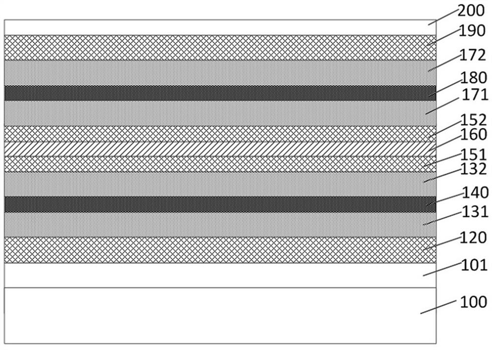
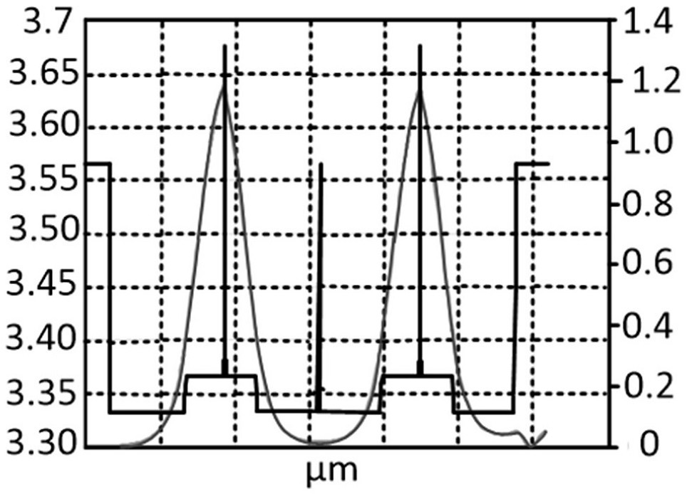
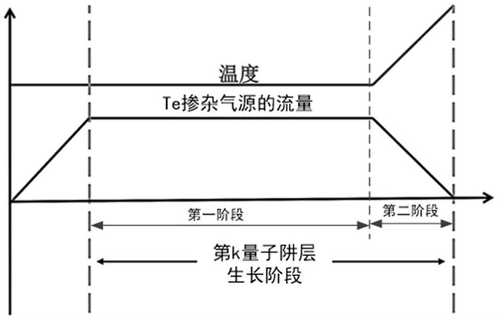
[0031] For semiconductor lasers, the increase in output power is generally achieved by increasing the injection current. For conventional quantum well semiconductor lasers with a single active region, the internal quantum efficiency is always less than 1. However, as the current increases, the power transmission wire required by the semiconductor laser needs to be thickened to reduce the resistance to maintain the reliability of the power supply. The use of dual active region semiconductor lasers can achieve nearly double the power output under a single injection current, achieving the purpose of reducing the working current. The epitaxial structure of the dual active region semiconductor laser is to stack two active regions vertically through one epitaxial growth, and the upper active region and the lower active region are connected in series through a reverse highly doped PN tunnel junction. After a carrier participates in recombination light emission through the first activ...


PUM

PropertyMeasurementUnit
thicknessaaaaaaaaaa
thicknessaaaaaaaaaa
thicknessaaaaaaaaaa

Abstract

A multi-active-region semiconductor structure and a preparation method thereof, the multi-active-region semiconductor structure comprising: a 2k-1 common confinement layer located between the kth active layer and the kth tunnel junction and in contact with the kth tunnel junction; The 2kth common confinement layer located between the k+1th active layer and the kth tunnel junction and in contact with the kth tunnel junction; the forbidden band width of the kth quantum well layer is smaller than the forbidden bandwidth of the kth first semiconductor layer Width and the bandgap width of the kth second semiconductor layer; the total thickness of the 2k-1 common confinement layer and the 2k common confinement layer is greater than the critical optical field coupling thickness and less than or equal to 2 times of the critical optical field coupling thickness; the second The thickness of the k quantum well layer is less than or equal to 1 / 10 of the 2k-1 common confinement layer, and the thickness of the k quantum well layer is less than or equal to 1 / 10 of the 2k common confinement layer. The luminous efficiency of the semiconductor structure with multiple active regions is effectively improved and the crosstalk of light field is reduced.

Description

technical field [0001] The invention relates to the technical field of semiconductors, in particular to a semiconductor structure with multiple active regions and a preparation method thereof. Background technique [0002] A light-emitting semiconductor device is a device that produces stimulated emission with a certain semiconductor material as a working substance. Its working principle is: through a certain excitation method, between the energy band (conduction band and valence band) of the semiconductor material, or Between the energy band of the material and the energy level of the impurity (acceptor or donor), the particle number inversion of the non-equilibrium carrier is realized. When a large number of electrons and holes in the particle number inversion state recombine, stimulated emission occurs Because of its small size and high electro-optical conversion efficiency, light-emitting semiconductor devices are widely used. [0003] At present, the existing technolog...

Claims


Application Information

Patent Timeline
Patent Type & Authority Patents(China)
IPC IPC(8): H01S5/343H01S5/34
CPCH01S5/343H01S5/34H01S2304/00
Inventor 王俊苟于单周立程洋谭少阳张立晨李波胡燚文闵大勇
Owner SUZHOU EVERBRIGHT PHOTONICS CO LTD
Why Eureka
Try Eureka