

Field electron emission device structure with reverse bias nano junction
A field electron emission and device structure technology, which is applied to electrical components, electrode devices and related components, cathode ray tubes/electron beam tubes, etc. volatility etc.
- Summary
- Abstract
- Description
- Claims
- Application Information
AI Technical Summary
Problems solved by technology
Method used
Image

Examples
Embodiment 1
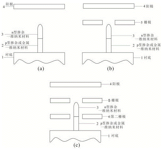
[0038] The preparation of the field electron emission device structure (single electrode, emitter: p-Si / n-ZnO) with the reverse bias nano-junction comprises the following steps:
[0039] S1. In P-type doping (10 19 cm -3 ) on the silicon wafer, using a magnetron sputtering deposition system to deposit a Zn seed layer with a thickness of 20 to 50 nm on its surface;
[0040] S2. Spin-coat electron beam photoresist (PMMA) with a thickness of about 500-650 nm;
[0041] S3. Using the electron beam exposure system to directly write the electron beam photoresist;
[0042] S4. developing the exposed sample to obtain a PMMA nanohole array template with a pitch of 4 μm, and the hole diameter is less than 200nm;
[0043] S5. Using the hydrothermal method (Zn 2+ 0.005mol / L, 80°C, 18h) to grow a one-dimensional ZnO nanostructure perpendicular to the substrate in the micropore, the method of growing ZnO refers to the patent application number 200710032889.1);
[0044] S6. Use ultrasoni...
Embodiment 2
[0049] The preparation of the field electron emission device structure (single electrode, emitter: p-Si / n-Si) with the reverse bias nano-junction comprises the following steps:
[0050] S1. Select the N-type doping (10 14 cm -3 ~10 18 cm -3 ) P-type doping of silicon semiconductor (10 19 cm -3 ~10 21 cm -3 ) a silicon semiconductor substrate, using a thin film deposition system to deposit a metal Cr layer with a thickness of about 50nm on its surface;
[0051] S2. Spin-coat negative electron beam photoresist (AR-N7520.18) with a thickness of about 400nm;
[0052] S3. Using an electron beam lithography system to perform pattern exposure on the photoresist;
[0053] S4. Develop the exposed sample by using a mixed solution of tetramethylammonium hydroxide (TMAH) and deionized water with a volume ratio of 4:1 to obtain a photoresist lattice pattern with a diameter of 100-200 nm;
[0054] S5. Using the photoresist lattice pattern as a mask, transfer the photoresist pattern...
Embodiment 3
[0060] The experimental method is the same as in Example 1 or 2, the only difference is that zinc oxide is replaced by N-type doped tin dioxide, ferric oxide, titanium oxide, tungsten oxide and other metal oxides or gallium nitride, indium phosphide, etc. any of the materials.
PUM
 Abstract
Description
Claims
Application Information