MOSFET structure and process for low gate induced drain leakage (GILD)

a mosfet and drain leakage technology, applied in the field of integrated circuits, can solve the problems circuit operation, and gidl problem, and achieve the effect of increasing the potential between the drain and the gate conductor

Inactive Publication Date: 2000-08-01
GLOBALFOUNDRIES INC
View PDF18 Cites 85 Cited by
  • Summary
  • Abstract
  • Description
  • Claims
  • Application Information

AI Technical Summary

Problems solved by technology

As device geometries shrink, reliability problems due to gate induced drain leakage (GIDL) force the integrated circuit to operate at voltages which are lower than desired for best performance.
Furthermore, the GIDL problem is exacerbated when DRAM array MOSFETS are operated at negative wordline low levels or with an opposite gate doping polarity (i.e. P+ gated N-type field effect transistor (NFET)) because such operating parameters increase the potential between the drain and the gate conductor.

Method used


Image

  • MOSFET structure and process for low gate induced drain leakage (GILD)
  • MOSFET structure and process for low gate induced drain leakage (GILD)
  • MOSFET structure and process for low gate induced drain leakage (GILD)

Examples


Embodiment Construction

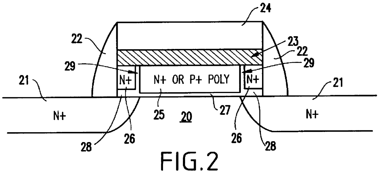
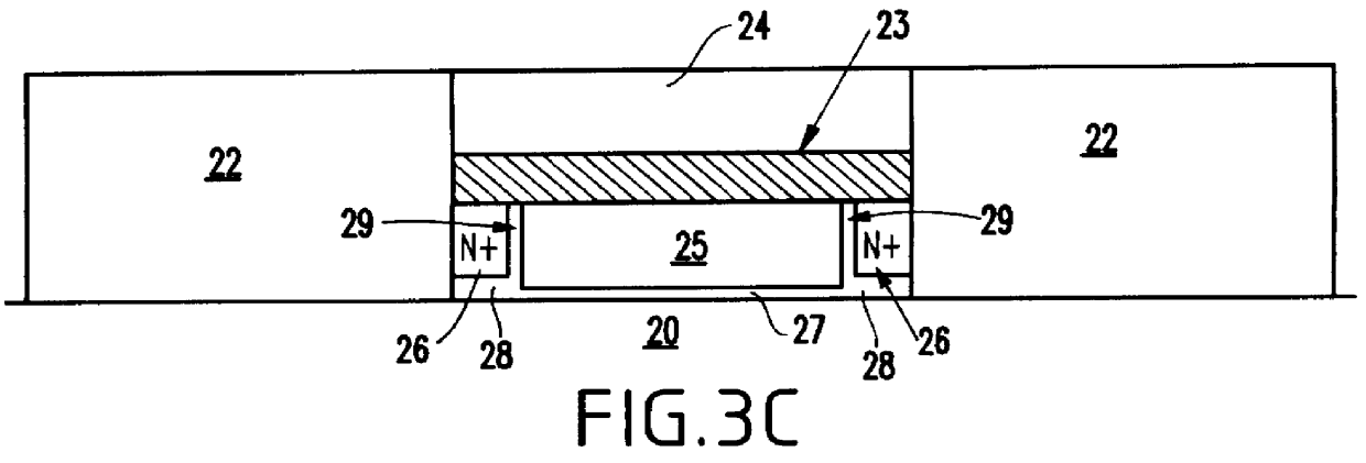
Referring now to FIG. 2, a preferred embodiment of the invention is illustrated. More specifically, the inventive structure includes a gate-channel region 20, source and drain regions 21, a gate dielectric layer 27, 28, a central gate conductor 25, outer (e.g., edge) gate conductors 26, a conductive layer 23, a cap 24 and insulating spacers 22. The structure is formed using various processes, such as those discussed below with respect to FIGS. 3A-4C.

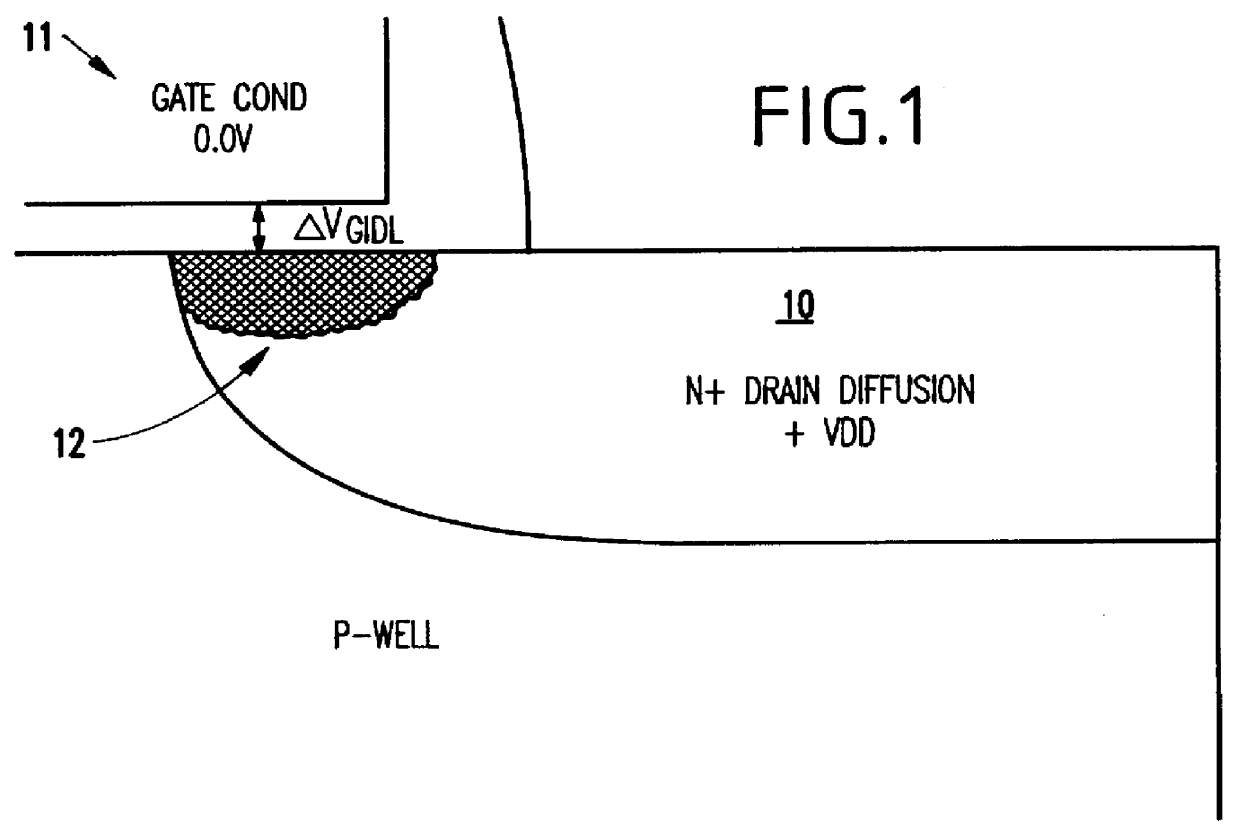
With the inventive outer gate conductors 26, the dielectric 27, 28 thickness can be increased in the area 28 where the source and drain 21 overlap the gate, which reduces gate induced drain leakage, and overlap capacitance. Further, the outer gate conductors 26 are somewhat insulated from the central gate conductor 25 by the gate dielectric 29, which further reduces the gate induced drain leakage problem discussed in the Background section. Thus, the inventive structure tailors the gate work function and / or the gate oxide thickness in th...


PUM


Abstract

A structure and method for forming a metal oxide semiconductor field effect transistor structure comprises, a substrate having a gate-channel region and source and drain regions adjacent the gate-channel region, a gate insulator over the substrate, a central gate conductor positioned above the gate-channel region and over the gate insulator and outer gate conductors over the gate insulator and adjacent the central gate conductor, wherein the gate insulator has a first thickness under the central gate conductor and a second thickness greater than the first thickness under the outer gate conductors. The center and outer gate conductors may consist of different material types (i.e., different work functions). The polarity of the source-drain doping is independent of the polarity of the central or outer gate conductors.

Description

1. Field of the InventionThe present invention generally relates to integrated circuits and more specifically to structures and methods for reducing gate induced drain leakage in semiconductor devices.2. Description of the Related ArtAs device geometries shrink, reliability problems due to gate induced drain leakage (GIDL) force the integrated circuit to operate at voltages which are lower than desired for best performance. Gate induced drain leakage results from the generation of electron-hole pairs in the surface the depletion region of a field effect transistor (FET) along the area where the gate conductor overlaps the drain diffusion region when the device is biased such that the drain potential is more positive (by greater than approximately 1V) than the gate potential.As shown in FIG. 1 it is necessary for a portion of the drain diffusion region 10 to be positioned under the gate conductor 11. Therefore, if the gate conductor were at 0 V and the drain diffusion region 10 were ...

Claims


Application Information

Patent Timeline
Patent Type & Authority Patents(United States)
IPC IPC(8): H01L21/28H01L29/66H01L29/49H01L29/423H01L21/336H01L21/02H01L29/40H01L29/78H01L29/51
CPCH01L21/28114H01L21/28167H01L29/42368H01L29/42376H01L29/4983H01L29/66583H01L29/7831H01L21/28211H01L29/512
Inventor MANDELMAN, JACK A.RADENS, CARL J.
Owner GLOBALFOUNDRIES INC
Why Eureka
Try Eureka