

Integrated circuit device and electronic instrument
Active Publication Date: 2007-01-04
SEIKO EPSON CORP
View PDF99 Cites 74 Cited by
- Summary
- Abstract
- Description
- Claims
- Application Information
AI Technical Summary
Problems solved by technology
Therefore, if the chip size is reduced by merely shrinking the integrated circuit device as the display d
Method used
View moreImage
Smart ImageViewing Examples

Examples
 PUM
 Abstract
An integrated circuit device includes a pad PDx and an electrostatic discharge protection element ESDx formed in a rectangular region and electrically connected with the pad PDx. The pad PDx is disposed in an upper layer of the electrostatic discharge protection element ESDx so that an arrangement direction of the pads is parallel to a long side direction of the region in which the electrostatic discharge protection element ESDx is formed, and the pad PDx overlaps part or the entirety of the electrostatic discharge protection element ESDx.
Description
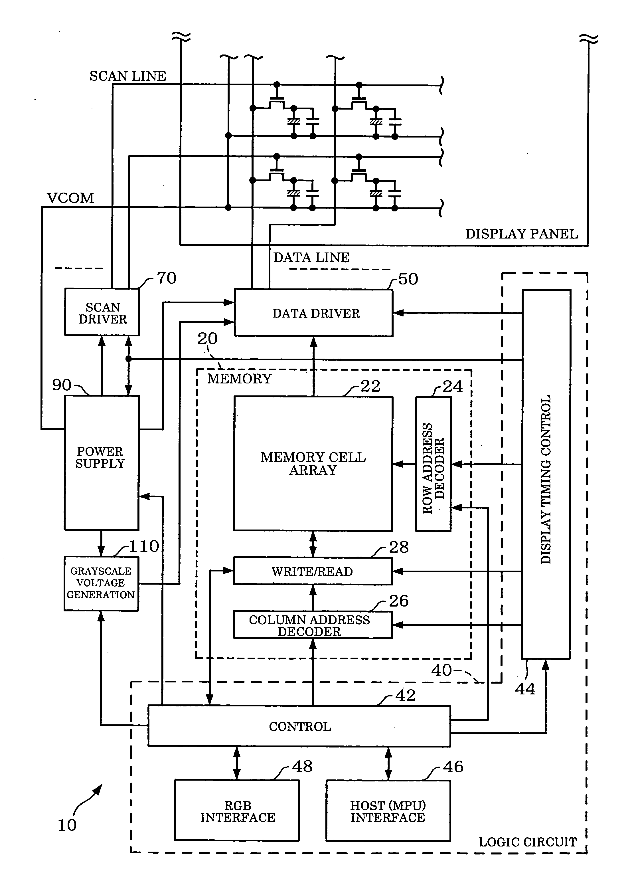
[0001] Japanese Patent Application No. 2005-192479 filed on Jun. 30, 2005 and Japanese Patent Application No. 2005-253390 filed on Sep. 1, 2005, are hereby incorporated by reference in their entirety. BACKGROUND OF THE INVENTION [0002] The present invention relates to an integrated circuit device and an electronic instrument. [0003] A display driver (LCD driver) is an example of an integrated circuit device which drives a display panel such as a liquid crystal panel (JP-A-2001-222249). A reduction in the chip size is required for the display driver in order to reduce cost. [0004] However, the size of the display panel incorporated in a portable telephone or the like is almost constant. Therefore, if the chip size is reduced by merely shrinking the integrated circuit device as the display driver by using a microfabrication technology, it becomes difficult to mount the integrated circuit device. SUMMARY [0005] A first aspect of the invention relates to an integrated circuit device com...
Claims
Login to View More Application Information
Patent Timeline
 IPC IPC(8): H02H9/00
CPCG02F1/13452G02F2202/28G09G2310/027G09G3/3696G09G2300/0426G09G3/3688G02F1/133
InventorKUMAGAI, TAKASHIISHIYAMA, HISANOBUMAEKAWA, KAZUHIROITO, SATORUFUJISE, TAKASHIKARASAWA, JUNICHIKODAIRA, SATORUSAIKI, TAKAYUKITAKAMIYA, HIROYUKI
OwnerSEIKO EPSON CORP