

Light emitting diode package
a technology of light-emitting diodes and sub-conductor modules, which is applied in the direction of transportation and packaging, vehicle spotlighting, mass transit vehicle lighting, etc., can solve the problems of b>10/b>, the wiring structure of the conventional light-emitting diodes suffers, and the manufacturing of a highly reliable light-emitting diode package with such a sub-sub-sub-sub-sub-sub-sub-sub-sub
- Summary
- Abstract
- Description
- Claims
- Application Information
AI Technical Summary
Benefits of technology
Problems solved by technology
Method used
Image

Examples
Embodiment Construction
[0023] Preferred embodiments of the present invention will now be described in detail with reference to the accompanying drawings.
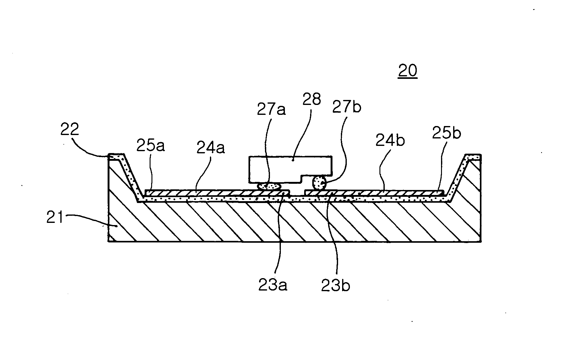
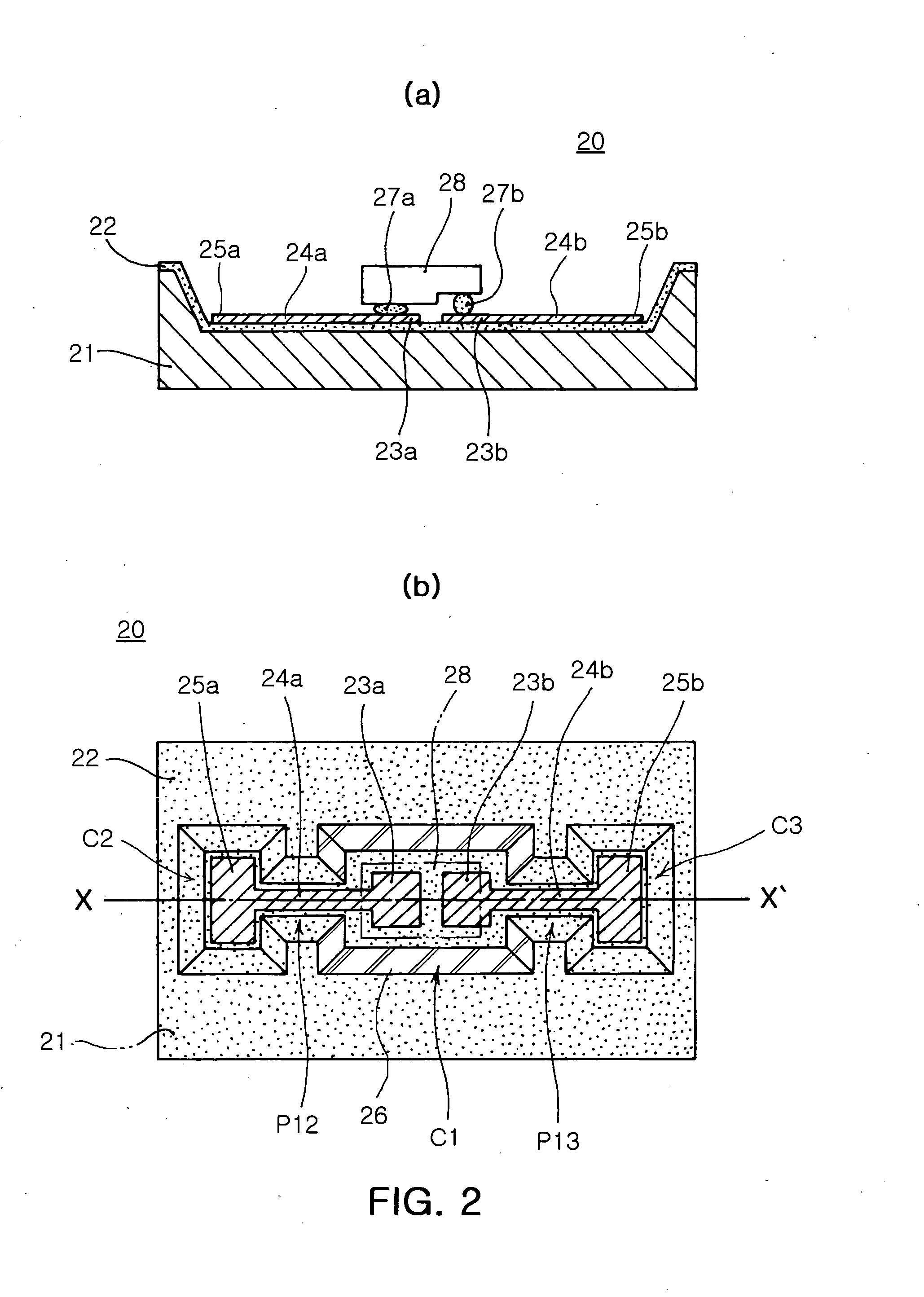
[0024]FIGS. 2a and 2b are a side sectional view and a plan view illustrating a light emitting diode package 20 in accordance with one embodiment of the invention, respectively. FIG. 2a shows a cross section taken along line X-X′ of the light emitting diode package 20 shown in FIG. 2b.
[0025] The light emitting diode package 20 of FIG. 2b comprises a submount substrate 21 having a main cavity C1 formed thereon. The submount substrate 21 may be a silicon substrate, which can be easily processed by MEMS. The main cavity C is provided as a mounting region, and has side walls inclined upwards. The inclined side walls of the mounting region are formed with reflecting plates 26 for enhancing light emitting efficiency of the light emitting diode 28, as shown in FIG. 2b. The reflecting plates 28 are composed of a highly reflective metal, such as Al or Ag.
[0026] ...
PUM
 Abstract
Description
Claims
Application Information