

Semiconductor package based on lead-on-chip architecture, the fabrication thereof and a leadframe for implementing in a semiconductor package
a technology of semiconductor packages and lead-on-chips, applied in the direction of solid-state devices, electric devices, basic electric elements, etc., can solve the problems of limited data storage capability and limited length of the chip extending orthogonally to the opposing sides of the package where the interconnecting leads are located, and achieve the effect of fast and low-cost process
- Summary
- Abstract
- Description
- Claims
- Application Information
AI Technical Summary
Benefits of technology
Problems solved by technology
Method used
Image

Examples
Embodiment Construction
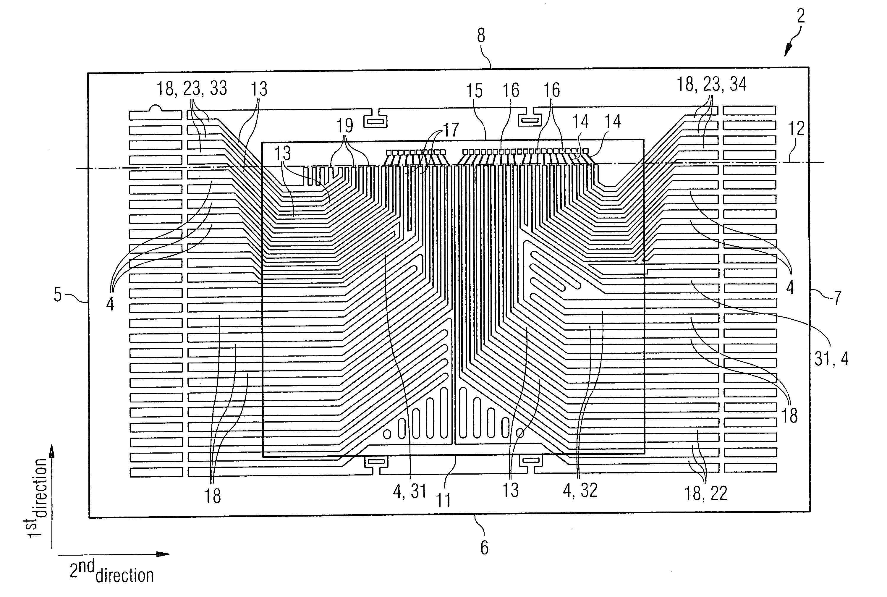
[0039]FIG. 1 depicts a plan view of a semiconductor device 1 according to one embodiment of the present invention. The semiconductor device 1 has a first side 27, a second side 29, a third side 28 and a fourth side 30. The first side 27 and the second side 29 are shorter than the third side 28 and the fourth side 30. The first side 27, the second side 29, the third side 28 and the fourth side 30 of the semiconductor form a rectangle.
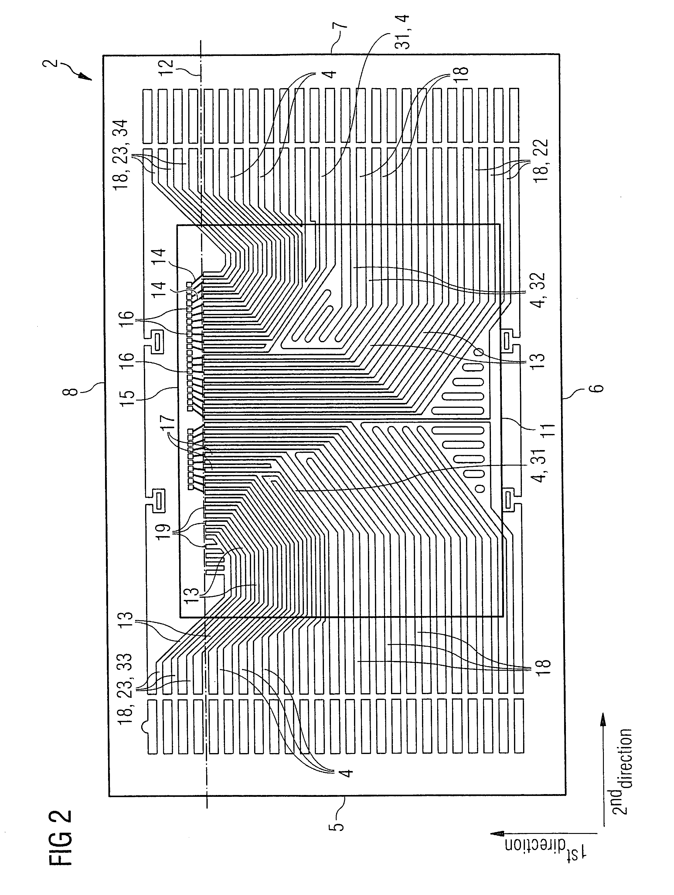
[0040] The semiconductor device 1 comprises a molded package 21. The surface of the molded package 21 is made of epoxy resulting from the injection molding at a stage of the fabrication process of the semiconductor device 1. A portion of a leadframe 2 (e.g., depicted in FIG. 2) is encapsulated by the molded package 21. Portions 26 of board level contact portions 18 of the leadframe 2 protrude from the first side 27 and from the second side 29 of the semiconductor device 1. The portions 26 of the board level contact portions 18 may be coated with a layer...
PUM
 Abstract
Description
Claims
Application Information