
Semiconductor package based on lead-on-chip architecture, the fabrication thereof and a leadframe for implementing in a semiconductor package

a technology of semiconductor packages and lead-on-chips, applied in the direction of solid-state devices, electric devices, basic electric elements, etc., can solve the problems of limited data storage capability and limited length of the chip extending orthogonally to the opposing sides of the package where the interconnecting leads are located, and achieve the effect of fast and low-cost process

Inactive Publication Date: 2008-03-25
POLARIS INNOVATIONS LTD
View PDF7 Cites 0 Cited by
  • Summary
  • Abstract
  • Description
  • Claims
  • Application Information

AI Technical Summary

Benefits of technology

"The present invention provides a semiconductor device and a method for fabricating it that allows for larger chips to be fitted into the semiconductor device. The semiconductor device comprises a chip and a leadframe with a multiplicity of leads that are arranged in a way that allows for the contacts of the chip to be connected to the leads of the leadframe. The leadframe has a middle section that connects the board level contact portions and the chip level contact portions, and the chip level contact portions align with a line extending along the second direction. The method for fabricating the semiconductor device involves placing the surfaces of the chip in proximity to the edges of the chip and aligning the contacts of the chip with the chip level contact portions of the leadframe. The chip and leadframe are then molded and the leadframe is removed to form a molded package. The semiconductor device is suitable for use in various applications such as automotive, aerospace, and defense."

Problems solved by technology

Therefore, the length of the side of the chip extending orthogonally to the opposing sides of the package where the interconnecting leads are located is limited.
Since the chip size determines the data storage capability of the chip, the data storage capability is also limited.

Method used


Image

  • Semiconductor package based on lead-on-chip architecture, the fabrication thereof and a leadframe for implementing in a semiconductor package
  • Semiconductor package based on lead-on-chip architecture, the fabrication thereof and a leadframe for implementing in a semiconductor package
  • Semiconductor package based on lead-on-chip architecture, the fabrication thereof and a leadframe for implementing in a semiconductor package

Examples


Embodiment Construction

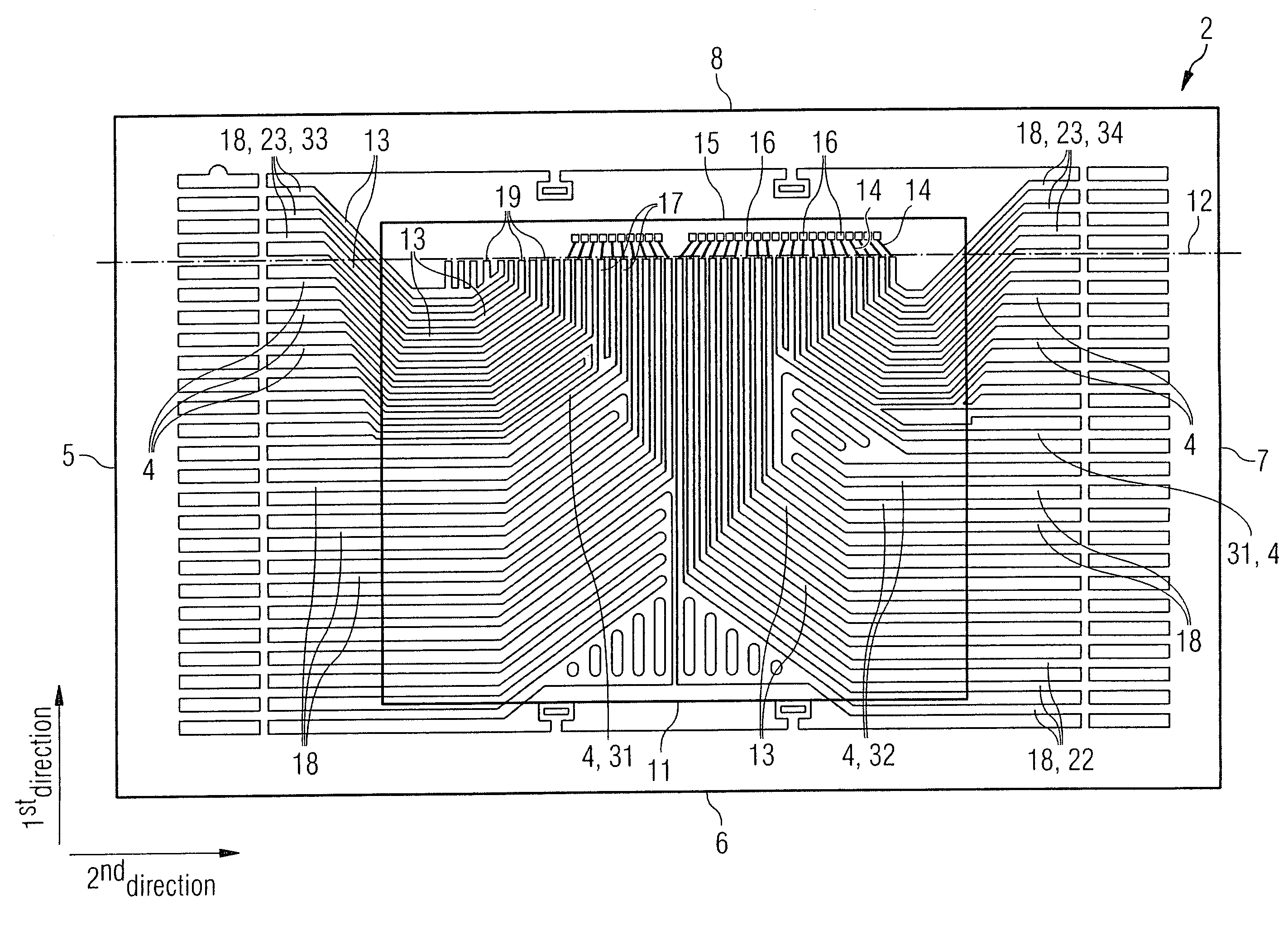
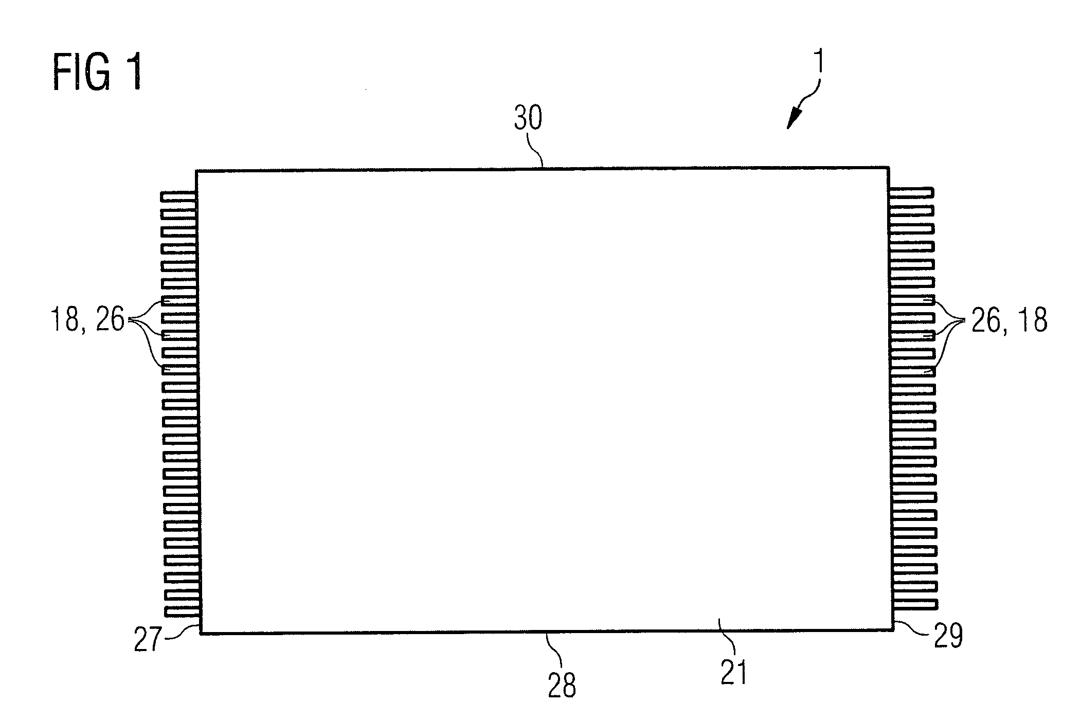
[0040]FIG. 1 depicts a plan view of a semiconductor device 1 according to one embodiment of the present invention. The semiconductor device 1 has a first side 27, a second side 29, a third side 28 and a fourth side 30. The first side 27 and the second side 29 are shorter than the third side 28 and the fourth side 30. The first side 27, the second side 29, the third side 28 and the fourth side 30 of the semiconductor form a rectangle.

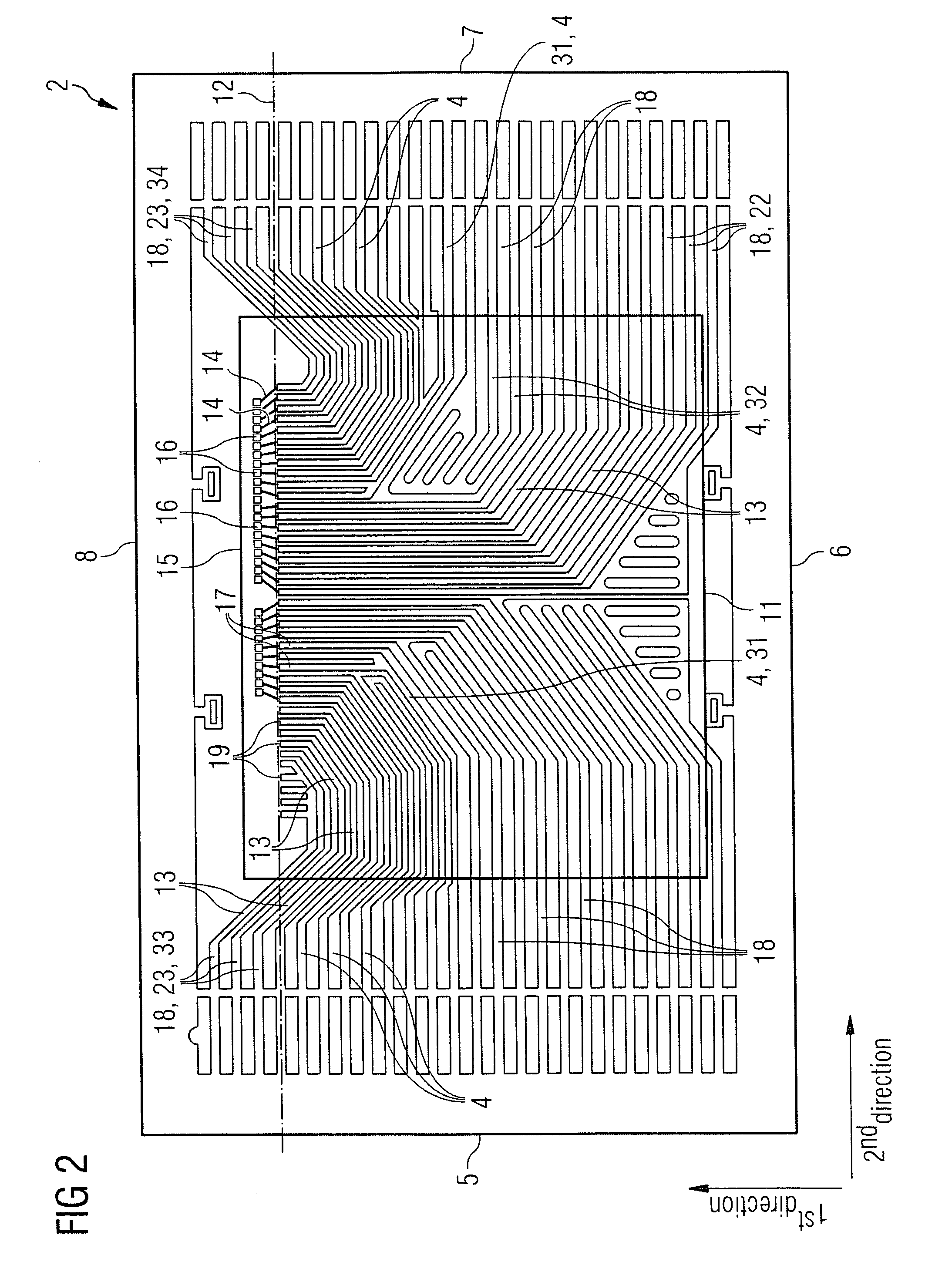
[0041]The semiconductor device 1 comprises a molded package 21. The surface of the molded package 21 is made of epoxy resulting from the injection molding at a stage of the fabrication process of the semiconductor device 1. A portion of a leadframe 2 (e.g., depicted in FIG. 2) is encapsulated by the molded package 21. Portions 26 of board level contact portions 18 of the leadframe 2 protrude from the first side 27 and from the second side 29 of the semiconductor device 1. The portions 26 of the board level contact portions 18 may be coated with a layer t...


PUM


Abstract

A leadframe includes a multiplicity of leads. The leads have a board level contact portion, an intermediate portion and a chip level contact portion. The intermediate portion is disposed between the board level contact portion and the chip level contact portion. The board level contact portions extend from one of the first side or the second side of the semiconductor device along a second direction. The chip level contact portions extend along the first direction. Ends of the chip level contact portions are aligned along a line extending along the second direction. This leadframe can be included with a semiconductor chip in a packaged integrated circuit.

Description

TECHNICAL FIELD[0001]The present invention relates generally to semiconductor devices and more particularly to semiconductor packages based on lead-on-chip architecture.BACKGROUND[0002]Several leadframe packages having an industry standard pin layout and specified length and width are commonly used to house DRAM devices. The packages comprise a leadframe having a plurality of leads that serve as support for the semiconductor chip. Bonding wires connect the bonding pads of the chip to interconnecting leads of the leadframe that protrude on opposing sides from the molding compound and allow data transfer of the chip with an external device. The wire bonds are typically thin gold wires having a significant inductance. Therefore, layouts are preferred in which the distance between the leadframe terminals and the bonding pads of the chip is minimized.[0003]Typically the bonding wires are located close to the interconnecting leads on opposing sides of the package. Therefore, the length of...

Claims


Application Information

Patent Timeline
Patent Type & Authority Patents(United States)
IPC IPC(8): H01L23/495
CPCH01L23/4951H01L23/49513H01L23/49551H01L23/49575H01L2224/32145H01L2224/48091H01L2224/48247H01L2224/4826H01L2224/73215H01L2225/06562H01L2924/01025H01L2924/01078H01L2924/01079H01L2924/1532H01L2924/30107H01L2924/00014H01L24/48H01L2224/45144H01L2924/00H01L24/45H01L2924/14H01L2924/181H01L2924/00015H01L2224/05599
Inventor DOSSI, ROBERTO
Owner POLARIS INNOVATIONS LTD
Learn More