Method of fabricating flash memory device having self-aligned floating gate

a technology of floating gate and flash memory, which is applied in the direction of semiconductor devices, basic electric elements, electrical appliances, etc., can solve the problems of reducing the overlay margin, affecting the same cell characteristics, and difficult to confirm intrinsic cell characteristics

Inactive Publication Date: 2007-02-01
SK HYNIX INC
View PDF6 Cites 11 Cited by
  • Summary
  • Abstract
  • Description
  • Claims
  • Application Information

AI Technical Summary

Benefits of technology

[0011] A method of fabricating a flash memory device having a SAFG according to an aspect of the invention includes the steps of forming an isolation layer in a semiconductor substrate having a cell region and a test pattern region, defining an active region, and forming a first polysilicon layer, which is self-aligned with the isolation layer, on the active region with the tunnel oxide layer interposed therebetween; forming a dielectric layer and a capping polysilicon layer on the entire surface; stripping the capping polysilicon layer and the dielectric layer formed on the test pattern region; forming a second polysilicon layer on the entire surface; etching the second polysilicon layer and the capping polysilicon layer formed in the cell region using a control gate etch mask, forming a control gate, and etching the second polysilicon layer and the first polysilicon layer formed in the test pattern region, forming a gate of a test transistor; and etching the dielectric layer and the first polysilicon layer of the cell region to form a floating gate.

Problems solved by technology

Recently, as the size of components in NAND flash memory devices has been reduced, overlay margin has been reduced due the limitations of the application of a minimum design rule between the isolation layer and the floating gate and the mask resolution capability.
This is very detrimental to same cell characteristics.
It is thus difficult to confirm intrinsic cell characteristics.
Therefore, bias of a floating gate of a selected cell cannot be transferred to the floating gate of the test transistor.
Accordingly, it is impossible to form the test transistor and it is also difficult to analyze the intrinsic property.
This makes it difficult to improve device characteristics.

Method used


Image

  • Method of fabricating flash memory device having self-aligned floating gate
  • Method of fabricating flash memory device having self-aligned floating gate
  • Method of fabricating flash memory device having self-aligned floating gate

Examples


Embodiment Construction

[0014] In the following detailed description, only certain exemplary embodiments of the invention are shown and described simply by way of illustration. As those skilled in the art will realize, the described embodiments may be modified in various ways, all without departing from the spirit or scope of the invention. Accordingly, the drawings and description are to be regarded as illustrative in nature and not restrictive. Like reference numerals designate like elements throughout.

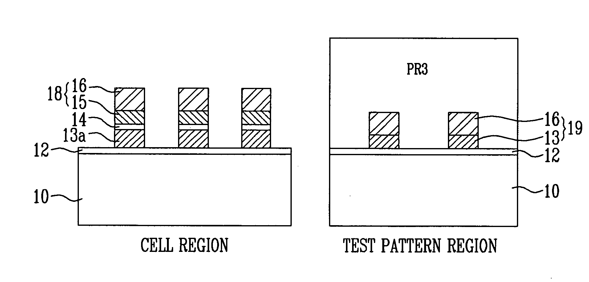
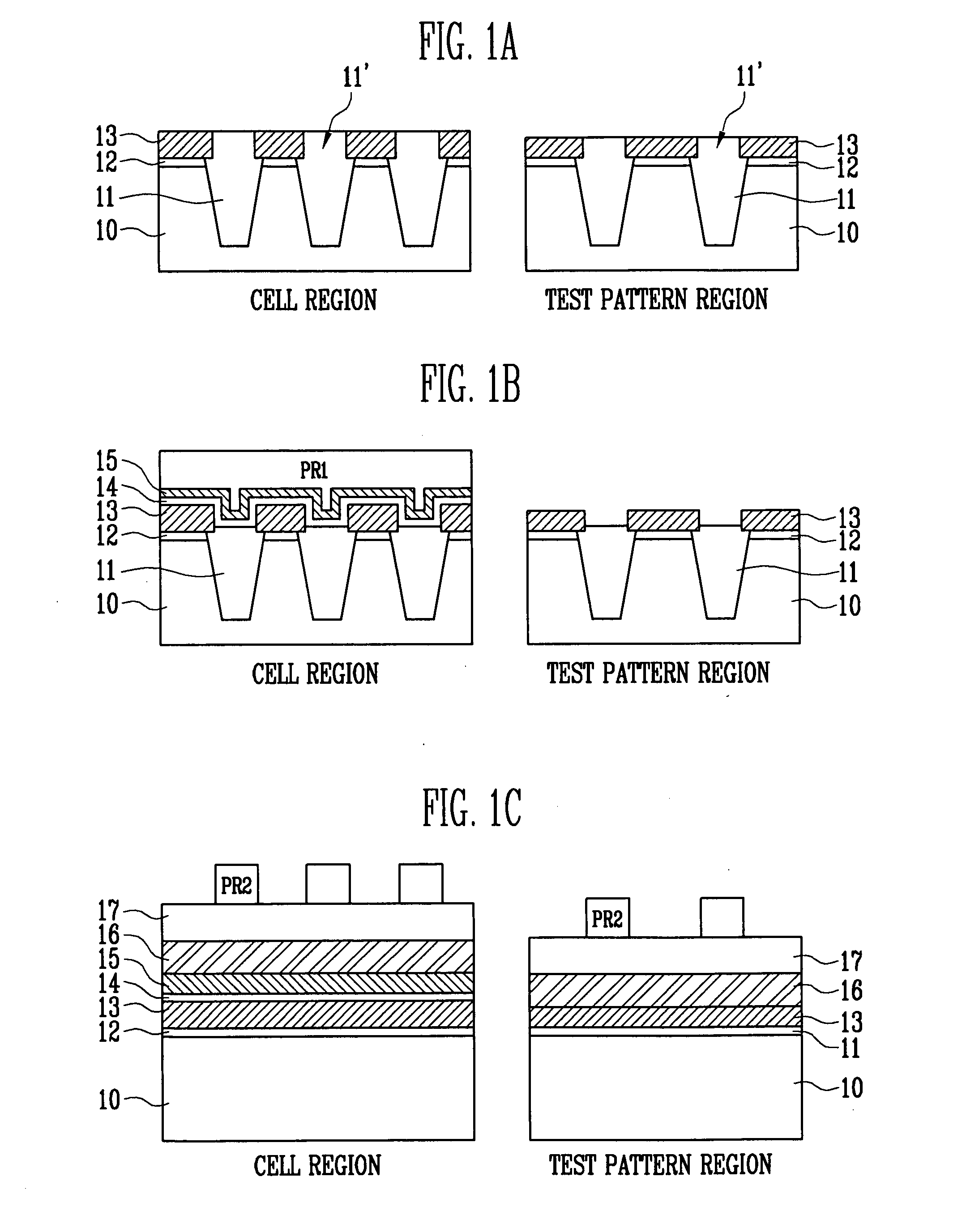
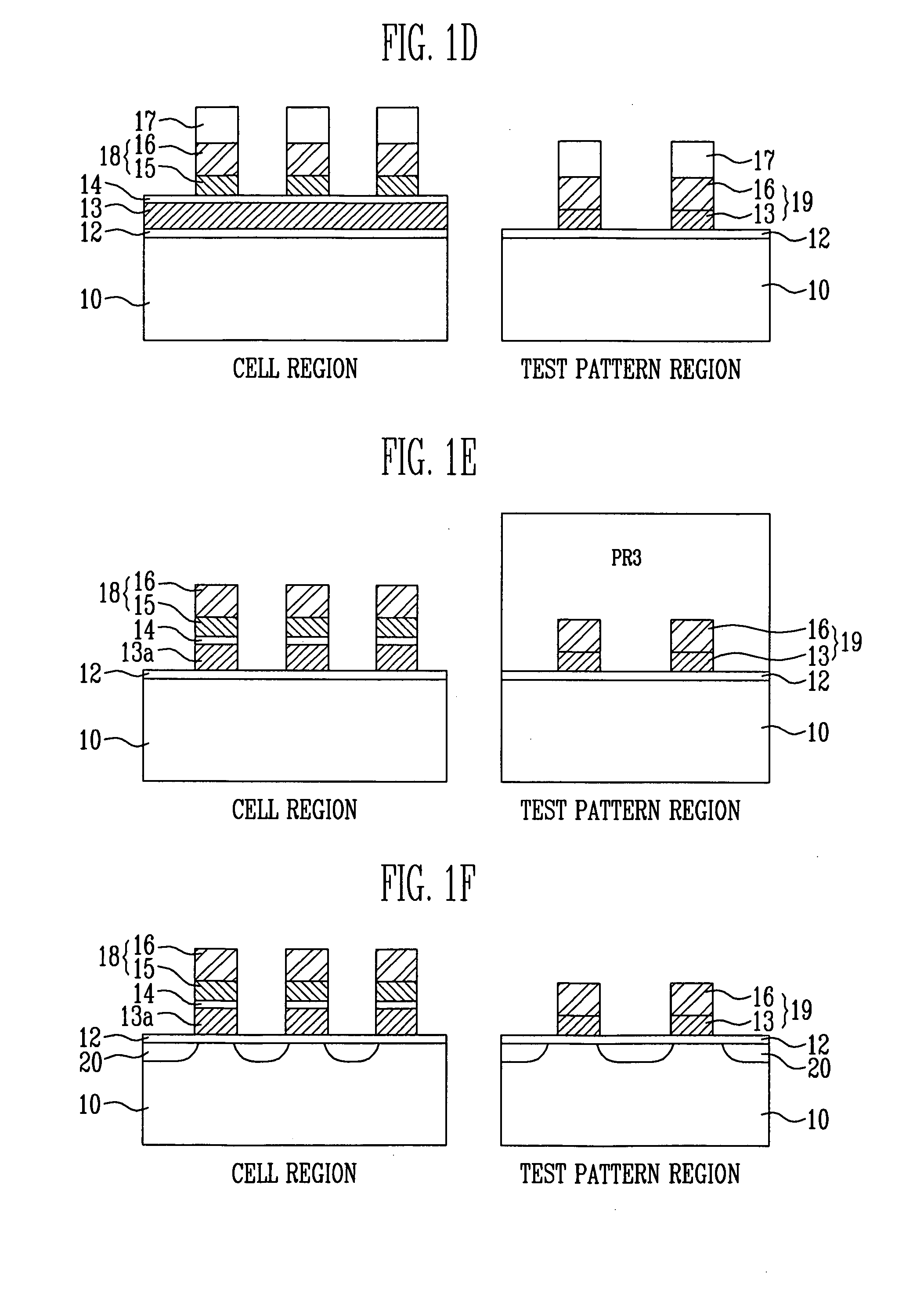
[0015]FIGS. 1A to 1F are cross-sectional views showing process steps of a method of fabricating flash memory device having an SAFG according to an embodiment of the invention. FIGS. 1A and 1B show the process steps in a word line direction and FIGS. 1C to 1F show the process steps in a bit line direction.

[0016] As shown in FIG. 1A, an isolation layer 11 is formed in a semiconductor substrate 10 having a cell region and a test pattern region, defining an active region. A tunnel oxide layer 12 is formed on...


PUM


Abstract

A method of fabricating a flash memory device having a self-aligned floating gate (SAFG) wherein a floating gate is formed by a SAFG process. After a dielectric layer is formed, the dielectric layer of a test pattern region is stripped and a control gate is formed so that the control gate and the floating gate are interconnected. Therefore, a test transistor can be formed even in the SAFG scheme.

Description

BACKGROUND [0001] 1. Field of the Invention [0002] The invention relates to a method of fabricating a flash memory device. More particularly, the invention relates to a method of fabricating a flash memory device, wherein a test transistor for analyzing cell characteristics is formed in a self-aligned floating gate (SAFG) scheme. [0003] 2. Discussion of Related Art [0004] Recently, as the size of components in NAND flash memory devices has been reduced, overlay margin has been reduced due the limitations of the application of a minimum design rule between the isolation layer and the floating gate and the mask resolution capability. This is very detrimental to same cell characteristics. [0005] To overcome the problem, a self-aligned floating gate (SAFG) scheme in which the floating gate is formed in the isolation trench, which is already formed on the substrate, in a self-aligned way has been introduced. [0006] In the flash cell, the floating gate serves as a memory that stores and e...

Claims


Application Information

Patent Timeline
Patent Type & Authority Applications(United States)
IPC IPC(8): H01L21/336H01L21/3205
CPCH01L27/105H01L27/11543H01L27/11526H10B41/40H10B41/48H10B99/00
Inventor LEE, YOUNG BOK
Owner SK HYNIX INC
Why Eureka
Try Eureka