

MRAM with super-paramagnetic sensing layer
- Summary
- Abstract
- Description
- Claims
- Application Information
AI Technical Summary
Benefits of technology
Problems solved by technology
Method used
Image

Examples
Embodiment Construction
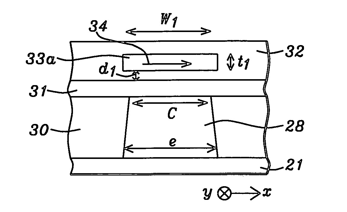
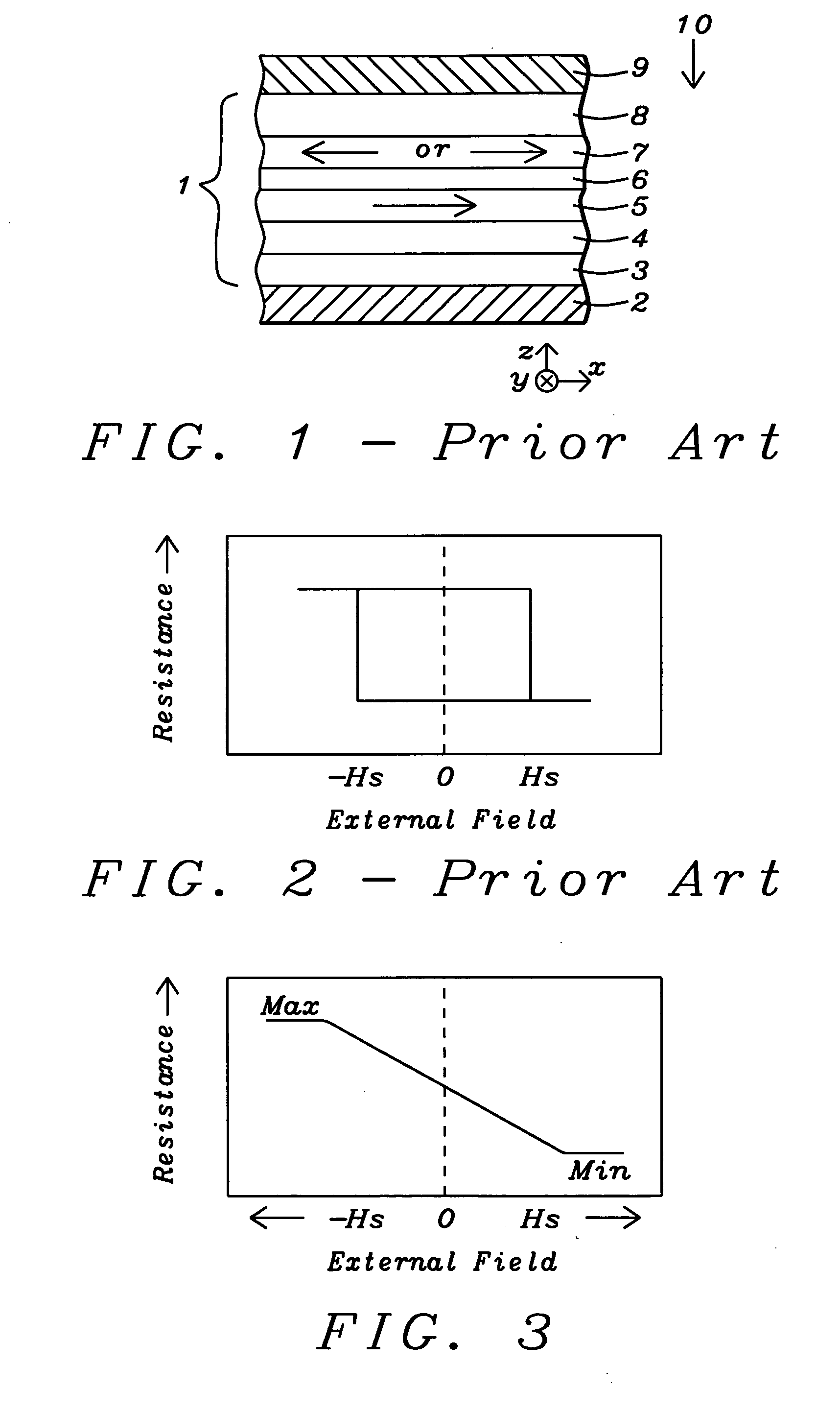
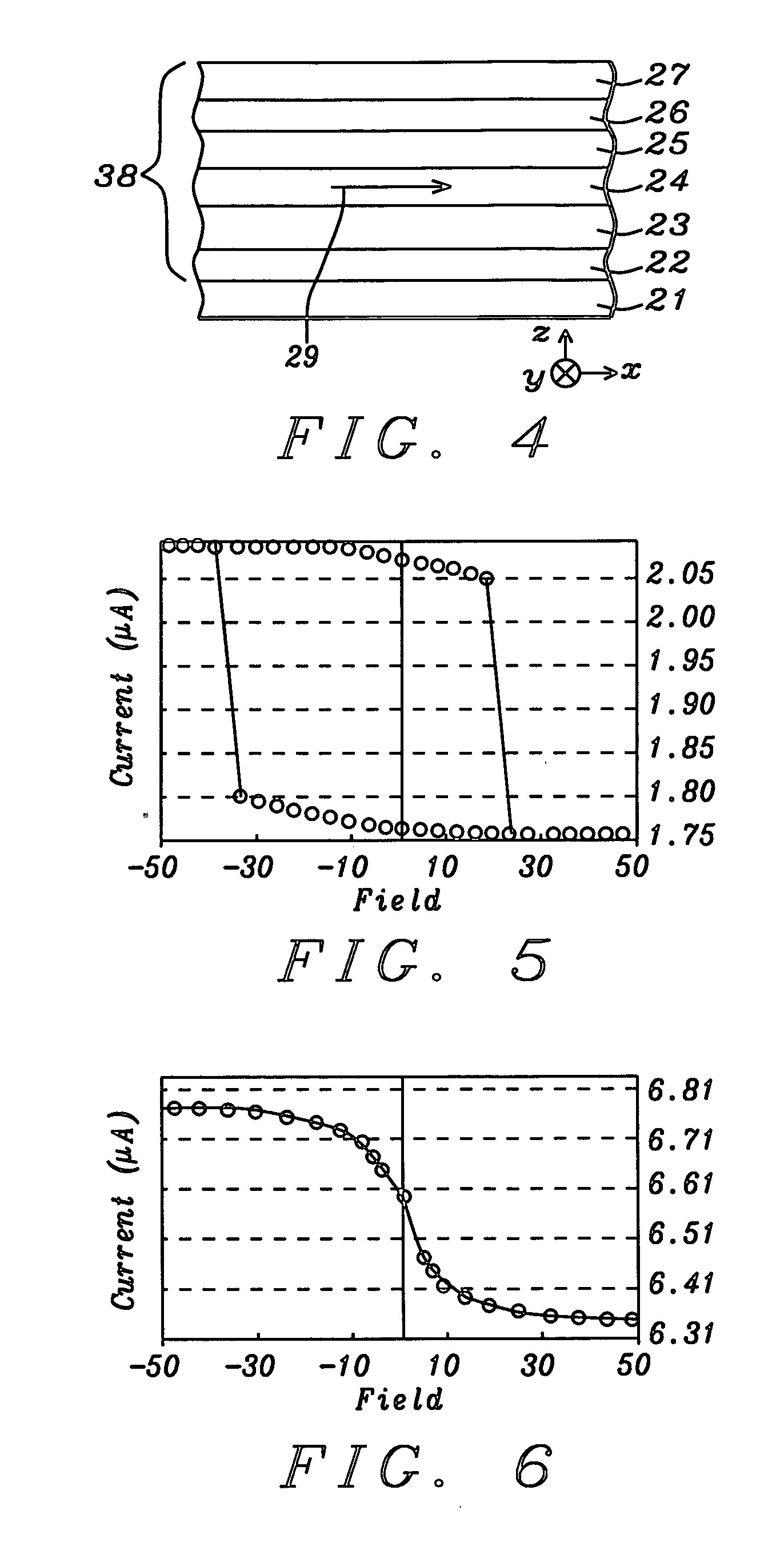
[0032] The present invention is a MRAM structure comprised of a MTJ having a ferromagnetic layer and a super-paramagnetic (SP) free layer that are separated by a tunneling layer in a pinned / tunnel / SP free configuration. The MRAM also includes a storage layer (for storing digital information) that is separated from the MTJ, disposed on the top surface of the MTJ, or formed at the bottom surface of the MTJ. The drawings are provided by way of example and are not intended to limit the scope of the invention. Note that only one MTJ is depicted in the drawings but it should be understood that there are a plurality of MTJs in an array that has multiple rows and columns in a memory device such as an MRAM chip. Furthermore, the MTJ may have a pinned / tunnel / SP free configuration or an SP free / tunnel / pinned configuration. The super-paramagnetic free layer has no (or very little) residual magnetization in the absence of an external field and has a magnetization substantially proportional to an...
PUM
 Abstract
Description
Claims
Application Information