
Method and apparatus for flag-less water bonding tool

a flag-less water bonding and tool technology, applied in the manufacture of basic electric elements, electrical equipment, semiconductor/solid-state device manufacturing, etc., can solve the problems of limiting the degree of integration of a given chip, conventional isolation techniques consume a considerable amount of valuable wafer surface area on the chip, and the technique is not free from limitations

Inactive Publication Date: 2007-04-19
SILICON GENERAL CORPORATION
View PDF5 Cites 72 Cited by
  • Summary
  • Abstract
  • Description
  • Claims
  • Application Information

AI Technical Summary

Benefits of technology

[0014] Various additional objects, features and advantages of the present invention can be more f

Problems solved by technology

These techniques, however, are not free from limitations.
For example, conventional isolation techniques consume a considerable amount of valuable wafer surface area on the chip, and often generate a non-planar surface as an artifact of the isolation process.
Either or both of these considerations generally limit the degree of integration achievable in a given chip.
Additionally, trench isolation often requires a process of reactive ion etching, which is extremely time consuming and can be difficult to achieve accurately.
Bulk silicon wafers, which are greater than 200 millimeters, are not free from defects and can reduce overall devices yields and the like.
Many problems, however, than have already been solved regarding fabricating devices on bulk silicon wafers remain to be solved for fabricating devices on epitaxial silicon wafers.
Epitaxial silicon wafers are made by way of epitaxial reactors, which are often expensive to purchase and difficult to maintain.
The process of forming epitaxial silicon is also slow and time consuming.
Accordingly, resulting epitaxial silicon wafers can often be expensive and cannot be used for the manufacture of many commercial or commodity devices such as dynamic random access memory devices (i.e., DRAMs), for example.

Method used


Image

  • Method and apparatus for flag-less water bonding tool
  • Method and apparatus for flag-less water bonding tool
  • Method and apparatus for flag-less water bonding tool

Examples


Embodiment Construction

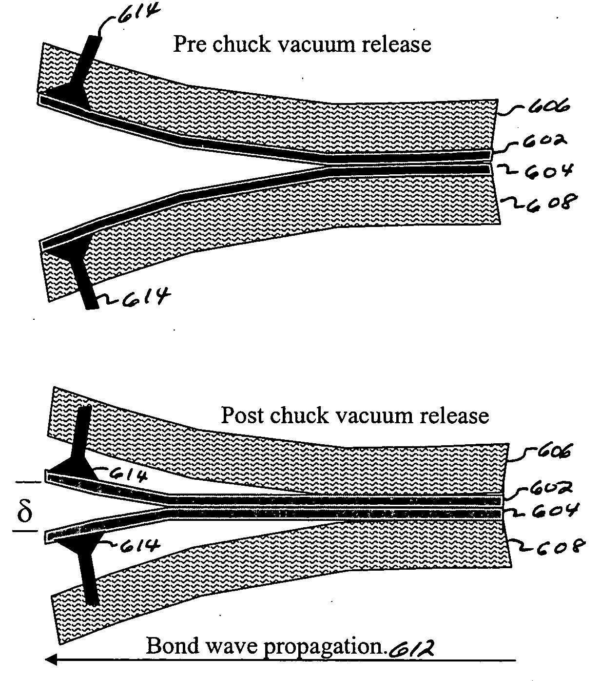
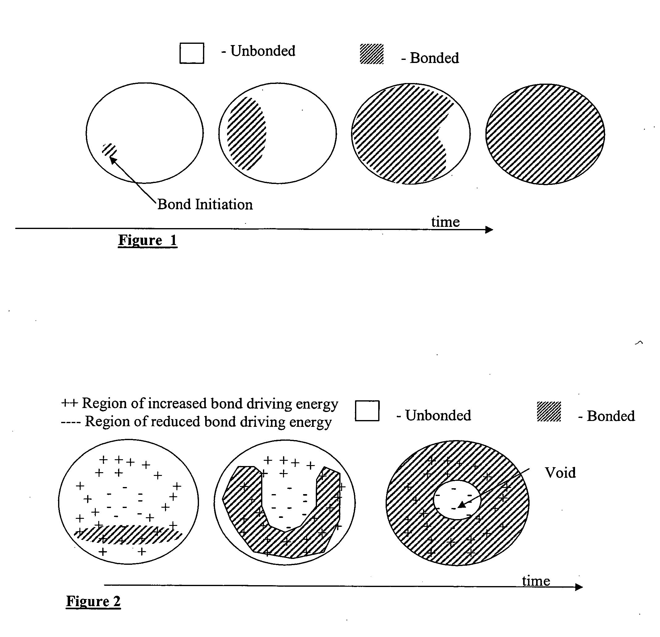
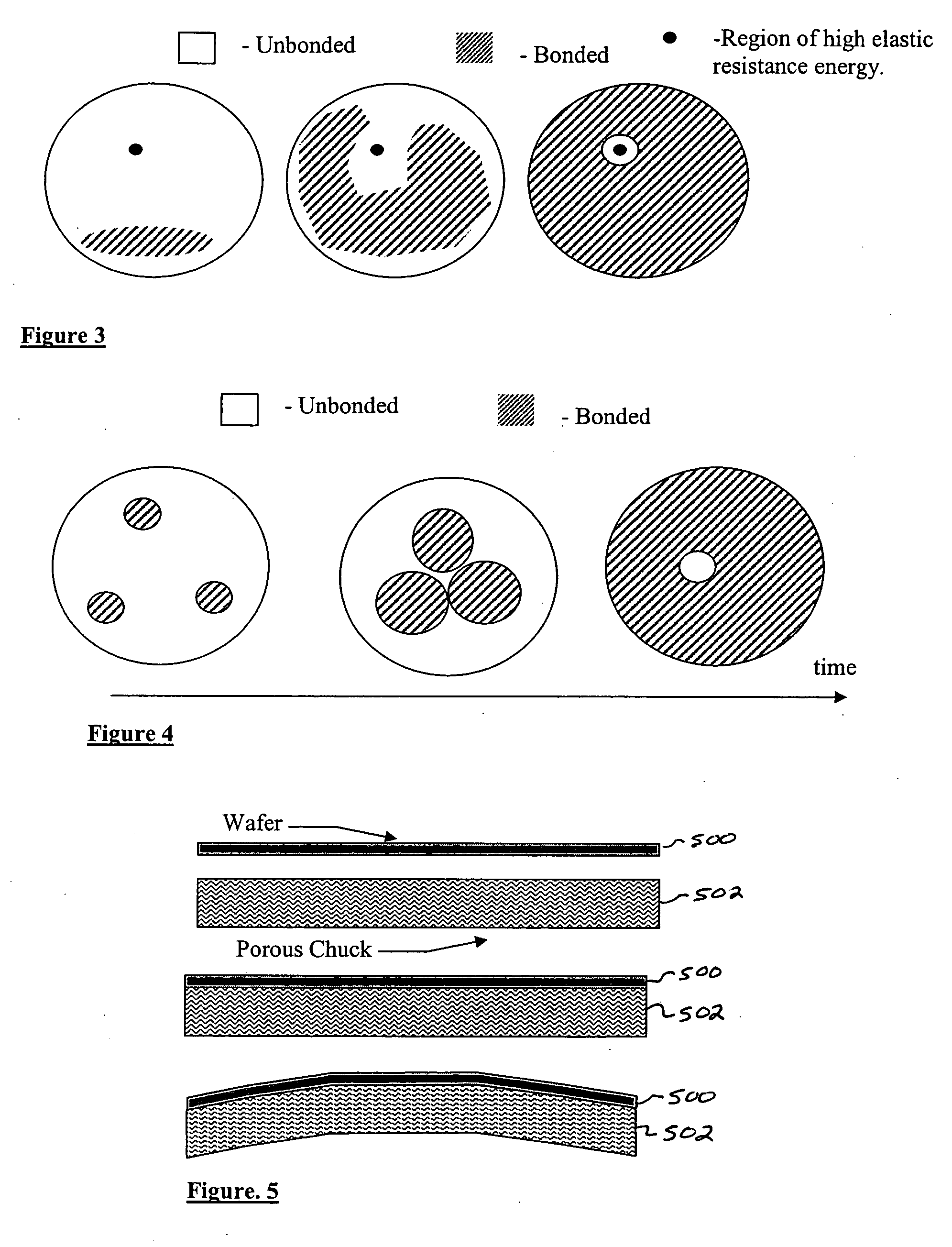
[0026] Embodiments in accordance with the present invention relate to methods and apparatuses for bonding together substrates in a manner that suppresses the formation of voids between them. In a specific embodiment, a backside of each substrate is adhered to a front area of flexible, porous chuck having a rear area in pneumatic communication with a vacuum. Application of the vacuum causes the chuck and the associated substrate to slightly bend. Owing to this bending, physical contact between local portions on the front side of the flexed substrates may be initiated, while maintaining other portions on front side of the substrates substantially free from contact with each other. A bond wave is formed and maintained at a determined velocity to form a continuous interface joining the front sides of the substrates, without formation of voids therebetween. In one embodiment, the chucks may comprise porous polyethylene sealed with polyimide except for a portion of the front configured to...


PUM


Abstract

Embodiments in accordance with the present invention relate to methods and apparatuses for bonding together substrates in a manner that suppresses the formation of voids between them. In a specific embodiment, a backside of each substrate is adhered to a front area of flexible, porous chuck having a rear area in pneumatic communication with a vacuum. Application of the vacuum causes the chuck and the associated substrate to slightly bend. Owing to this bending, physical contact between local portions on the front side of the flexed substrates may be initiated, while maintaining other portions on front side of the substrates substantially free from contact with each other. A bond wave is formed and maintained at a determined velocity to form a continuous interface joining the front sides of the substrates, without formation of voids therebetween. In one embodiment, the chucks may comprise porous polyethylene sealed with polyimide except for a portion of the front configured to be in contact with the substrate, and a portion of the backside configured to be in communication with a vacuum source.

Description

CROSS-REFERENCE TO RELATED APPLICATION [0001] The instant nonprovisional patent application claims priority to U.S. Provisional Patent Application No. 60 / 727,142, filed Oct. 14, 2005 and incorporated by reference herein for all purposes.BACKGROUND OF THE INVENTION [0002] The present invention relates to the manufacture of substrates. More particularly, the invention provides a technique including a method and device for bonding a first substrate to a second substrate for the manufacture of semiconductor integrated circuits, for example. But it will be recognized that the invention has a wider range of applicability; it can also be applied to other substrates for multi-layered integrated circuit devices, three-dimensional packaging of integrated semiconductor devices, photonic devices, piezoelectronic devices, microelectromechanical systems (“MEMS”), sensors, actuators, solar cells, flat panel displays (e.g., LCD, AMLCD), biological and biomedical devices, and the like. [0003] Integr...

Claims


Application Information

Patent Timeline
IPC IPC(8): H01L21/30H01L21/46
CPCH01L21/187H01L21/2007H01L21/67092
Inventor KIRK, HARRY R.HENLEY, FRANCOIS J.ONG, PHILIP JAMES
Owner SILICON GENERAL CORPORATION
Features
  • Generate Ideas
  • Intellectual Property
  • Life Sciences
  • Materials
  • Tech Scout
  • Unparalleled Data Quality
  • Higher Quality Content
  • 60% Fewer Hallucinations
Learn More