Double-sided etching method using embedded alignment mark

Inactive Publication Date: 2007-06-07
SAMSUNG ELECTRONICS CO LTD
View PDF4 Cites 1 Cited by
  • Summary
  • Abstract
  • Description
  • Claims
  • Application Information

AI Technical Summary

Benefits of technology

[0007] The present invention provides a double-sided etching method using a new embedded alignment mark that can reduce an alignment error in a Micro Electro-Mechanical Systems (MEMS) structure.

Problems solved by technology

However, the formation of alignment marks on the two surfaces causes a large alignment error, which results in a misalignment between comb electrodes in the MEMS structure, thus causing a failure of the MEMS device.

Method used


Image

  • Double-sided etching method using embedded alignment mark
  • Double-sided etching method using embedded alignment mark
  • Double-sided etching method using embedded alignment mark

Examples


Embodiment Construction

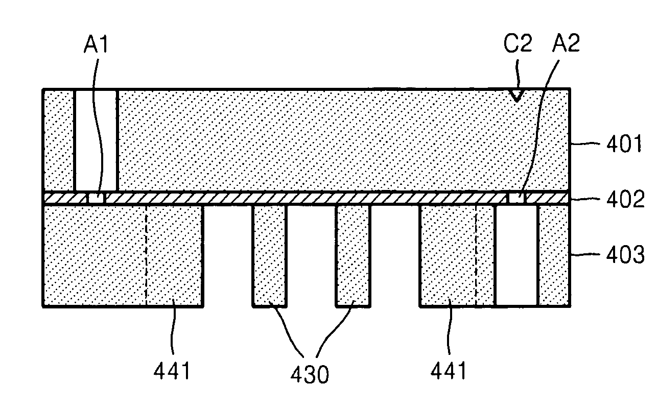
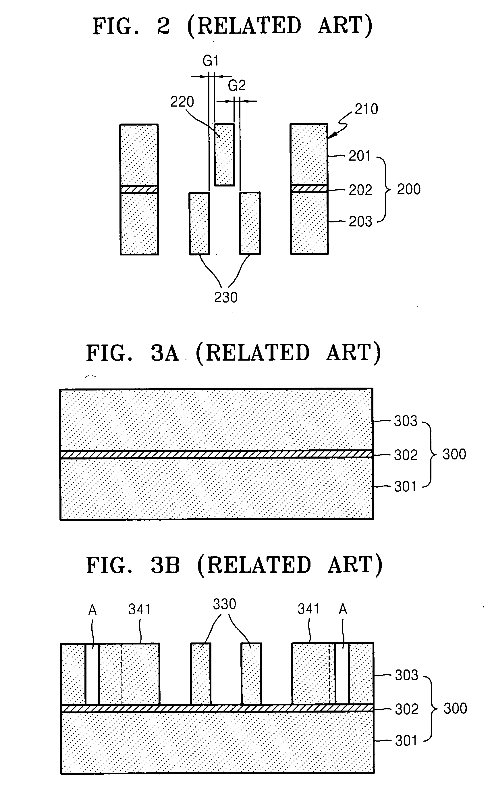
[0017] A double-sided etching method using an embedded alignment mark according to an exemplary embodiment of the present invention will now be described with reference to the accompanying drawings. In the drawings, some elements may be exaggerated for clarity or omitted to avoid complexity and to aid in the understanding of the present invention. This is not intended to limit the technical scope of the present invention.

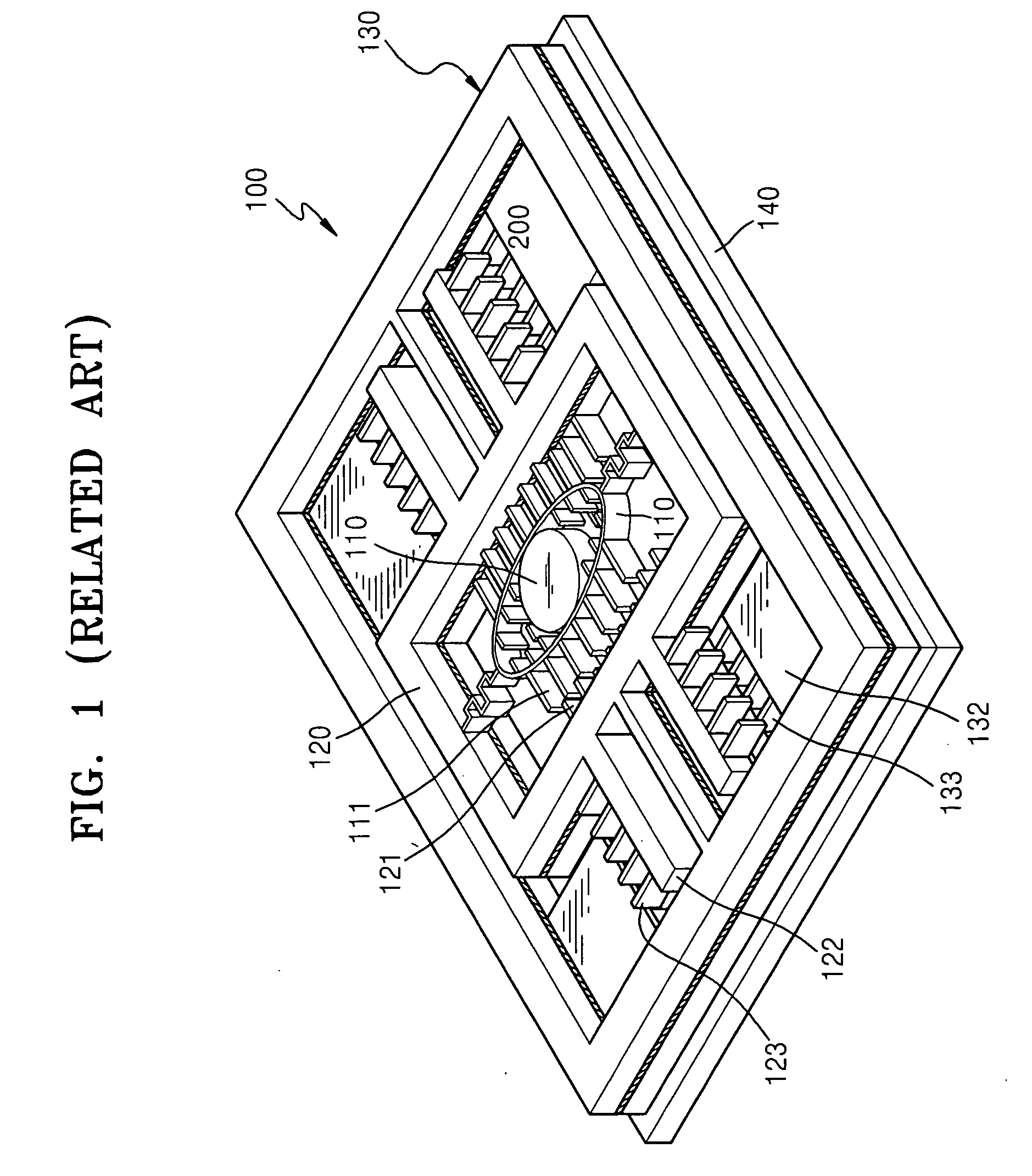
[0018]FIG. 1 is a perspective view of an optical scanner 100 disclosed in Korean Patent Application No. 2004-83537.

[0019] Referring to FIG. 1, the optical scanner 100 is actuated in two directions by first movable comb electrodes 111 and first stationary comb electrodes 121, which are disposed between a stage 110 and a movable frame 120, and second movable comb electrodes 123 and second stationary comb electrodes 133, which are disposed between a first member 122 extending from the movable frame 120 and a second member 132 extending from a stationary frame 130. Th...


PUM


Abstract

A double-sided etching method using an embedded alignment mark includes: preparing a substrate having first and second alignment marks embedded in an intermediate portion thereof; etching an upper portion of the substrate so as to expose the first alignment mark from a first surface of the substrate; etching the upper portion of the substrate using the exposed first alignment mark; etching a lower portion of the substrate so as to expose the second alignment mark from a second surface of the substrate; and etching the lower portion of the substrate using the exposed second alignment mark.

Description

CROSS-REFERENCE TO RELATED PATENT APPLICATIONS [0001] This application claims priority from Korean Patent Application No. 10-2005-0116636, filed on Dec. 1, 2005, in the Korean Intellectual Property Office, the disclosure of which is incorporated herein in its entirety by reference. BACKGROUND OF THE INVENTION [0002] 1. Field of the Invention [0003] Methods consistent with the present invention relate to a method of manufacturing a Micro Electro-Mechanical Systems (MEMS) structure and, more particularly, to a method of double-sided etching using an embedded alignment mark. [0004] 2. Description of the Related Art [0005] When manufacturing a MEMS structure such as an optical scanner for a flat panel display, double-side etching may be required. Thus, corresponding alignment marks are required for etching first and second surfaces. However, the formation of alignment marks on the two surfaces causes a large alignment error, which results in a misalignment between comb electrodes in the...

Claims


Application Information

Patent Timeline
IPC IPC(8): H01L21/76H01L21/302
CPCB81B2201/033B81C1/00547B81C1/00603
Inventor KO, YOUNG-CHULJEONG, HYUN-KU
Owner SAMSUNG ELECTRONICS CO LTD
Why Eureka
Try Eureka