Eureka AIR delivers breakthrough ideas for toughest innovation challenges, trusted by R&D personnel around the world.

Wafer bonding dynamic calibration method and device

A dynamic calibration and wafer bonding technology, applied in semiconductor/solid-state device manufacturing, semiconductor/solid-state device testing/measurement, electrical components, etc. and other problems, to achieve the effect of improving the wafer bonding accuracy and reducing the alignment error

Pending Publication Date: 2022-06-03
BEIJING U PRECISION TECH
View PDF1 Cites 0 Cited by
  • Summary
  • Abstract
  • Description
  • Claims
  • Application Information

AI Technical Summary

Problems solved by technology

When the position of the alignment mark on a batch of wafers is not in line with the calibration position of the device, or the distance between the two marks is different, during the alignment process of this batch of wafers, the alignment mark identification The device moves from the current position to the position of the calibration mark for calibration, and then moves to the recognition position of the alignment mark of the wafer, which will introduce additional motion errors, and it is very easy to introduce large errors during the nanoscale control process.
[0006] At present, only the patent CN201880000756.2 reduces the error by compensating during the alignment process, and has not yet found a method for the error caused by the movement of the alignment mark recognition position

Method used


Image

  • Wafer bonding dynamic calibration method and device
  • Wafer bonding dynamic calibration method and device
  • Wafer bonding dynamic calibration method and device

Examples


Embodiment Construction

[0031] The described embodiments of the present invention will be described below with reference to the accompanying drawings. As those of ordinary skill in the art would realize, the described embodiments may be modified in various different ways or combinations thereof, all without departing from the spirit and scope of the present invention. Accordingly, the drawings and description are illustrative in nature and are not intended to limit the scope of protection of the claims. Furthermore, in this specification, the drawings are not drawn to scale, and the same reference numerals refer to the same parts.

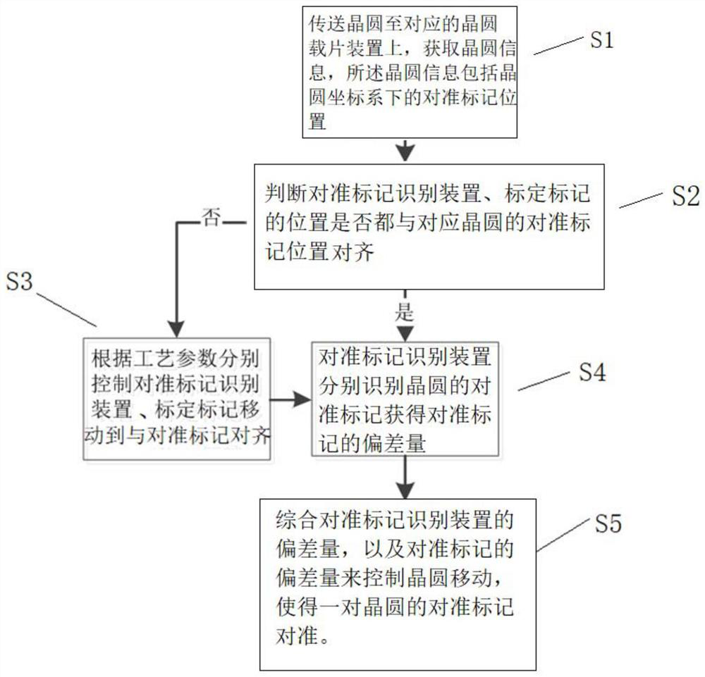
[0032] The wafer bonding dynamic calibration method in this embodiment is used to align a pair of wafers arranged one above the other, such as figure 1 shown, including:

[0033] In step S1, the wafer is transferred to obtain wafer information, where the wafer information includes an alignment mark position of the wafer. Transferring the wafer refers to transferring th...


PUM


Abstract

The invention discloses a wafer bonding dynamic calibration method and device, and the method comprises the steps: transmitting a wafer to a corresponding wafer slide device, and obtaining wafer information which comprises an alignment mark position under a wafer coordinate system; whether the positions of the alignment mark recognition device and the calibration mark are aligned with the alignment mark position of the corresponding wafer or not is judged, if not, the alignment mark recognition device and the calibration mark are controlled to move to be aligned with the alignment mark of the corresponding wafer, and then the deviation value of the alignment mark recognition device is calibrated through the calibration mark; the alignment mark recognition device recognizes the alignment marks of the wafers respectively to obtain deviation values of the alignment marks, and controls the wafers to move by integrating the deviation values of the alignment mark recognition device and the deviation values of the alignment marks, so that the alignment marks of the pair of wafers are aligned. According to the invention, the calibration mark and the alignment mark identification device are synchronously moved to the same position of the alignment mark in advance, so that the alignment error can be greatly reduced, and the wafer bonding precision is improved.

Description

technical field [0001] The present invention relates to the technical field of semiconductor manufacturing, and in particular, to a method and device for dynamic calibration of wafer bonding. Background technique [0002] With the increasing integration of semiconductor integrated circuits, it is more and more difficult to improve the integration of transistors in two-dimensional semiconductor chips. Therefore, in order to improve the integration density of transistors in semiconductor chips and reduce external leads, multilayer Stacked 3D integrated circuits. The emergence of three-dimensional integrated circuits breaks through the limitations of existing integrated circuits in terms of physics and materials. Three-dimensional integrated circuits are multi-layer planar devices that are stacked; the vertical interconnection between multiple chips is achieved through the bonding process during the manufacturing process. , which increases the space of the chip and improves th...

Claims


Application Information

Patent Timeline
IPC IPC(8): H01L21/68H01L21/66H01L21/67
CPCH01L21/681H01L22/12H01L22/20H01L21/67259
Inventor 赵雄峰张豹
Owner BEIJING U PRECISION TECH
Why Eureka
Eureka Blog
Learn More