Method and system for increasing yield of vertically integrated devices

Inactive Publication Date: 2007-06-07
FARIS SADEG M
View PDF7 Cites 41 Cited by
  • Summary
  • Abstract
  • Description
  • Claims
  • Application Information

AI Technical Summary

Benefits of technology

[0038] Accordingly, a primary object of the present invention is to provide a low cost three-dimensional integrated circuit.
[0039] An additi

Problems solved by technology

This approach allows only very limited vertical integration into the third dimension.
Unfortunately, the billion dollar costs are also well known to down-size the transistors one generation further and such transition process has also been hindered by technological difficulties, e.g., inability to smoothly integrate low-k dielectrics to reduce RC delay which is critical for submicron technologies.
If the devices are thinned and stacked on top of each other, the advantages in cost and circuit density are potentially huge.
Current methods all have limitations with respect to package size, cost, reliability and yield impact.
However, it is obvious that this technology is only a short-time solution because there is no revolutionary improvement.
The density of the devices is strictly limited to few layers.
Comparing with the package stacking, this method can reduce the dimension of IC stacks, but still cannot fully meet the challenge of 3D integration, since only packaging process and materials on each die can be saved in this technology.
Obviously this technology is time-consumption and high risk to damage the ICs during etching or grinding process.
However, this reference teaches a method that may be prohibitively expensive and severally functionally limited.
A key disadvantage of the method taught in the aforementioned U.S. Pat. No. 6,335,501 is that the applicants thereof note that forming three-dimension circuits on a wafer scale leads to low yield.
Further, alignment of each chip is considered to be a significant problem preventing wafer scale stacking.
Other disadvantages relate to the number of sequential repeated process steps.
These drawbacks lead to several disadvantages related to cost and functionality.
Cost detriments are found with the grinding removal; numerous sequential steps; chip scale as opposed to wafer scale stacking, wherein wafer scale is known to reduce cost; inability to overcome yield issues on wafer scale thus reverting to chip scale; limitation of the number of layers, thus to form higher number stacks, stacks must be stacked on other stacks; overall yield is decreased because the number of sequential statistically dependant through interconnects; multiple reflow steps potentially damage other layers.
Functionality drawbacks include lack of diagnostics; lack of interconnect versatility; limited space for interconnects; limited addressability of large stack, particularly memory stack; no ability to integrate noise shielding; no ability to integrate heat dissipation; no ability of ground plane; limitation of the number of layers.
The individual stacking and interconnection of die, along with the requirement for KGD causes this to be a very expensive manufacturing method.
Since accumulative surface roughness affects deposition of high quality polysilicon, the number of device layers is very limited.
Due to the nature of continuous growth, previously deposited layers have to undergo thermal cycles during fabrication of top device layers and device quality is affected.
Also due to these factors, application of this approach is limited only to the fabrication of rather simple devices, i.e., one-time programmable memory.
One primary deficiency is due to yield loss.
The processing is expensive and the yield loss for the stack is the compounded yield loss for each device in the layer.
The increased yield loss is sometimes tolerated for inexpensive devices such as SRAM stacks.
The process is very expensive and the applications have been limited to high end users, such as military and satellite technology.
Another deficiency of conventional vertical integration is due to the fact that the technology is limited to a die-scale.
The high cost of handling and testing individual die restricts these methods to high-end applications.
Another problem known throughout conventional manufacturing processes forming circuits is the requirement to support the processing device on a substrate.
Such tech

Method used


Image

  • Method and system for increasing yield of vertically integrated devices
  • Method and system for increasing yield of vertically integrated devices
  • Method and system for increasing yield of vertically integrated devices

Examples


Example

DETAILED DESCRIPTION OF THE DRAWINGS

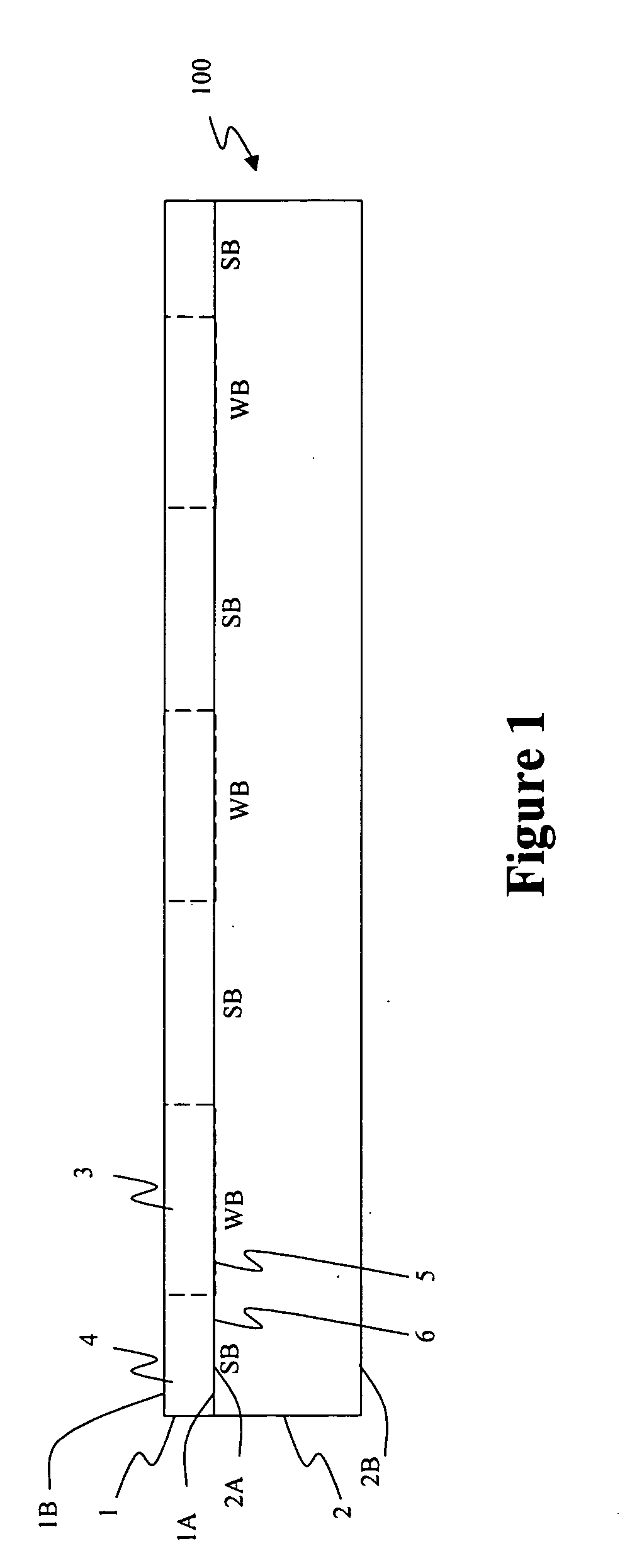
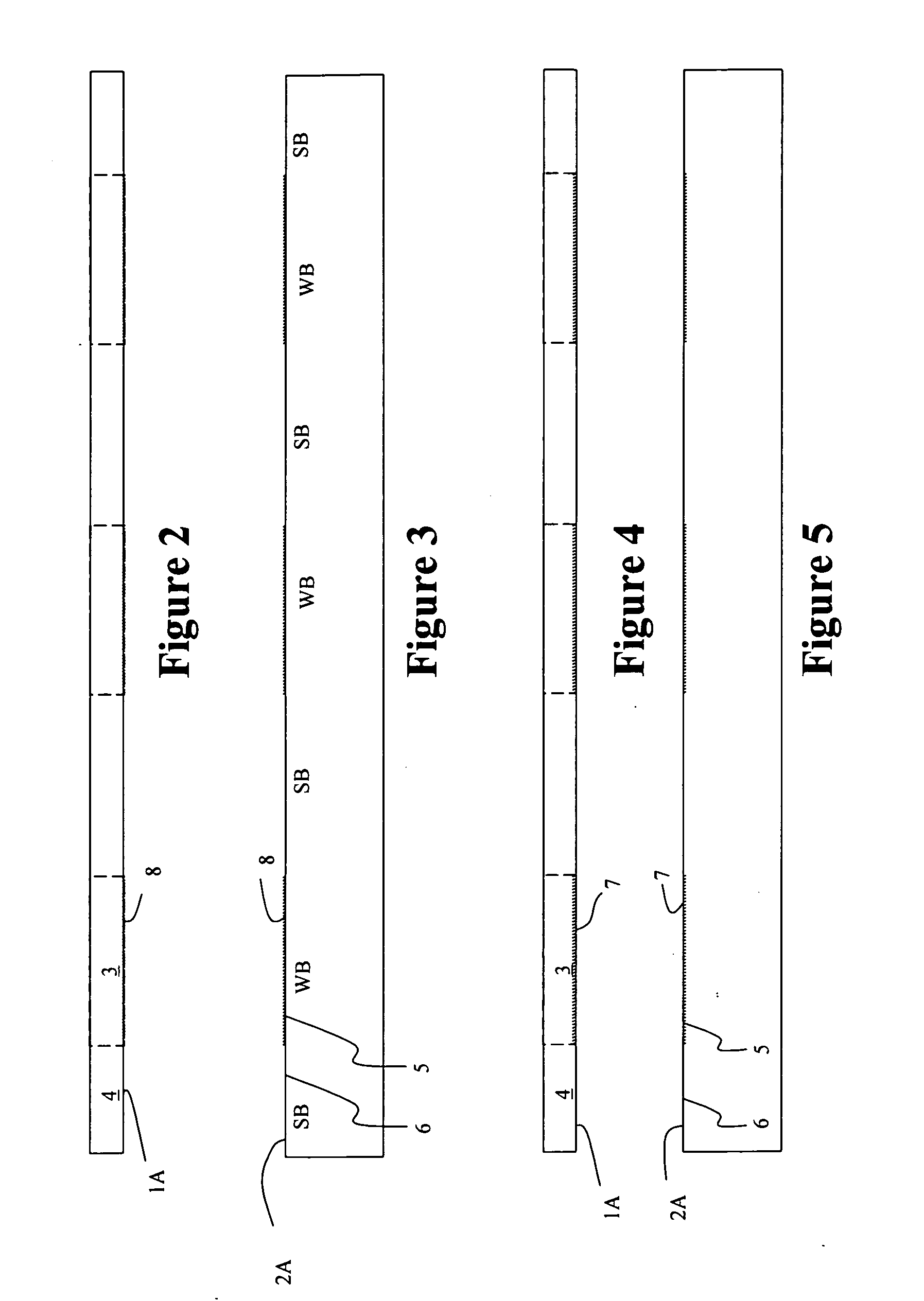
[0150] The present invention is related to forming three-dimensional integrated circuits. Prior to discussion of specific formation of these three-dimensional integrated circuits, a discussion of the starting substrates is presented, as set forth in Applicant's copending U.S. patent application Ser. No. 09 / 950,909 filed on Sep. 12, 2001 entitled “Thin films and Production Methods Thereof.” This substrate, referred to as a selectively bonded multiple layer substrate, allows for processing of multiple chips on a wafer as is known, but allows the chip layer of the wafer to be readily removed, preferably without mechanical grinding or other etch-back techniques. This chip layer then may be stacked on another chip layer, as described hereinafter, or alternatively, the chip layer may be diced into individual chips and stacked.

[0151] Referring to FIG. 1, a selectively bonded multiple layer substrate 100 is shown. The multiple layer substrate 100 includ...


PUM


Abstract

A method for increasing the manufacturing yield for a vertically integrated device is disclosed. The devices are composed of one or more multiple layer die. The number of functioning layers of each multiple layer die is determined diagnostically. Each of said multiple layer die are sorted based on said number of functioning layers. Also disclosed are methods for combining sorted die, and methods for slicing sorted die, to form die with a desired number of known good layers.

Description

CROSS-REFERENCE TO RELATED APPLICATIONS [0001] This application claims the benefit under 35 U.S.C. §119(e) of U.S. Provisional Application No. 60 / 689,169 filed Jun. 10, 2005 entitled “Method and System for Increasing Yield of Vertically Integrated Devices”, and is a continuation-in-part of and claims the benefit under 35 U.S.C. §120 of copending U.S. patent application Ser. No. 11 / 441,831 filed on May 26, 2006 which is a continuation of and claims the benefit under 35 U.S.C. §120 of U.S. patent application Ser. No. 11 / 077,542 entitled “Method And System For Increasing Yield Of Vertically Integrated Devices”, which is a continuation-in-part of and claims the benefit under 35 U.S.C. §120 of copending U.S. patent application Ser. No. 09 / 950,909 filed on Sep. 12, 2001 entitled “Thin Films and Production Methods Thereof” which are herein incorporated by reference.TECHNICAL FIELD [0002] The invention relates to a method and system for increasing manufacturing yield of vertical integrated ...

Claims


Application Information

Patent Timeline
IPC IPC(8): H01L21/30
CPCH01L21/6835H01L21/76254H01L24/03H01L24/05H01L24/06H01L24/80H01L24/94H01L24/98H01L25/0652H01L25/0657H01L25/50H01L2224/0557H01L2224/05624H01L2224/13009H01L2224/13021H01L2224/13025H01L2224/131H01L2224/24145H01L2224/8383H01L2224/83894H01L2225/06541H01L2225/06551H01L2225/06589H01L2225/06596H01L2924/01002H01L2924/01005H01L2924/01013H01L2924/01014H01L2924/01015H01L2924/01029H01L2924/01042H01L2924/01049H01L2924/0105H01L2924/01051H01L2924/01073H01L2924/01074H01L2924/01078H01L2924/01079H01L2924/01082H01L2924/01322H01L2924/014H01L2924/05042H01L2924/10158H01L2924/10329H01L2924/14H01L2924/1433H01L2924/15311H01L2924/30105H01L2924/3025H01L2224/9202H01L2924/01006H01L2924/01019H01L2924/01023H01L2924/01033H01L2924/01072H01L2924/0132H01L24/83H01L2224/0401H01L2924/13091H01L2924/0002H01L2924/1305H01L2924/00014H01L2924/01007H01L2924/01022H01L2924/01032H01L2924/01016H01L2924/0103H01L2924/01031H01L2924/3512H01L2924/00H01L2224/05552H01L24/24H01L24/81H01L2224/32145H01L2224/81815H01L2224/83862H01L2224/83874H01L2224/94H01L2924/00011H01L2224/81H01L2224/82H01L2224/83H01L2224/83205
Inventor FARIS, SADEG M.
Owner FARIS SADEG M
Why Eureka
Try Eureka