Semiconductor integrated circuit

Active Publication Date: 2007-07-26
KIOXIA CORP
View PDF7 Cites 18 Cited by
  • Summary
  • Abstract
  • Description
  • Claims
  • Application Information

AI Technical Summary

Problems solved by technology

On the other hand, an increase of storage capacity of the NAND-type flash memory becomes a problem as the function of the electronic apparatus increases.
Similarly, such problem occurs to a semiconductor memory with a large memory capacity in addition to the NAND-type flash memory.

Method used


Image

  • Semiconductor integrated circuit
  • Semiconductor integrated circuit
  • Semiconductor integrated circuit

Examples


embodiment

2. Embodiment

[0038]Next, there will be described an embodiment using a NAND-type flash memory as an example.

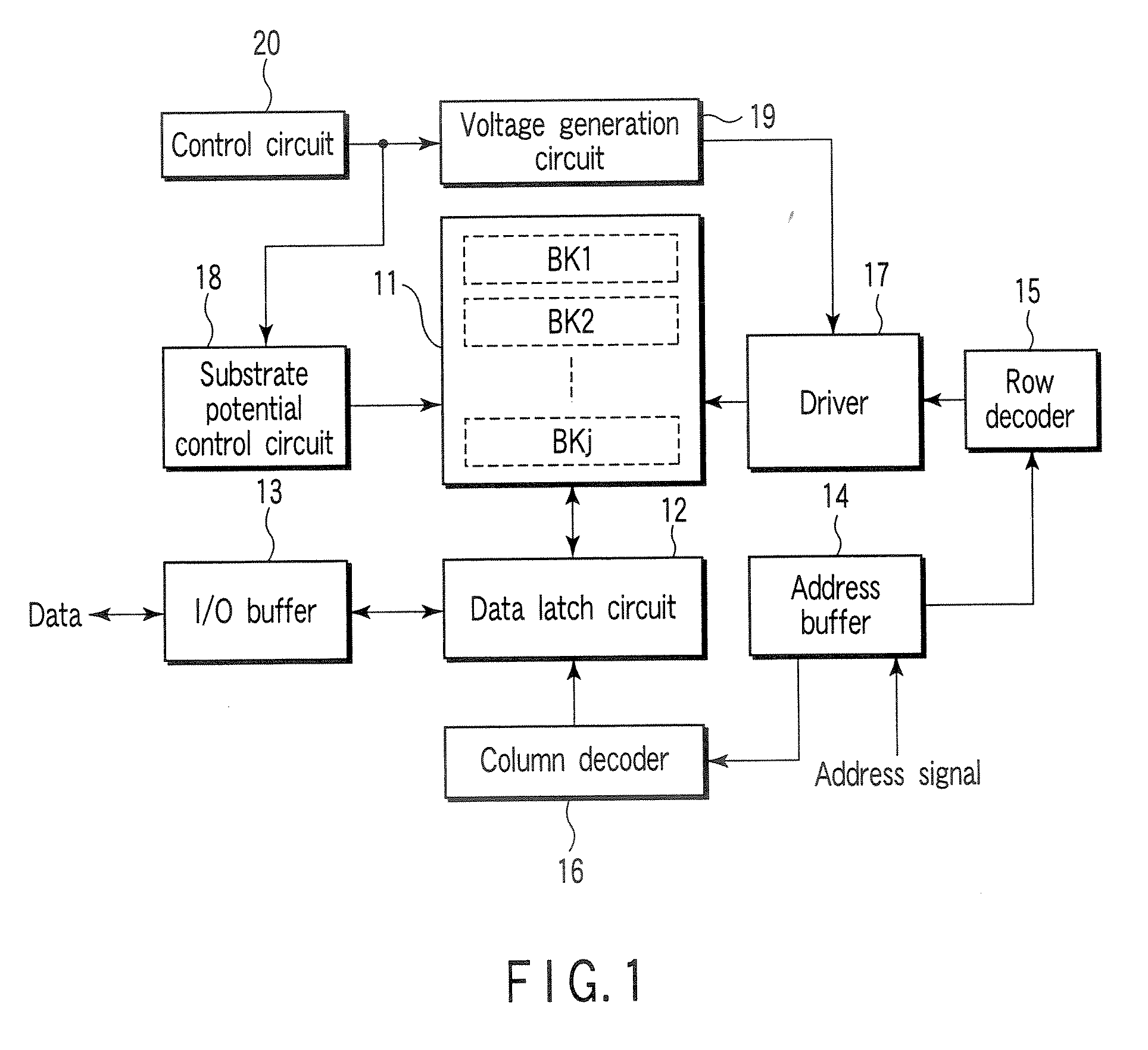
[0039](1) General Figure

[0040]FIG. 1 shows a general figure of a NAND-type flash memory.

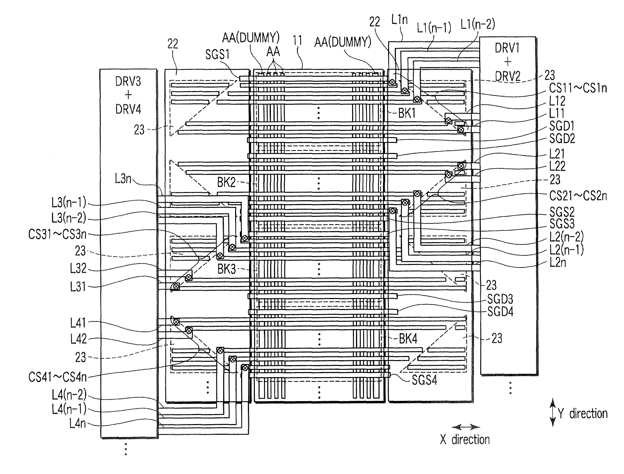
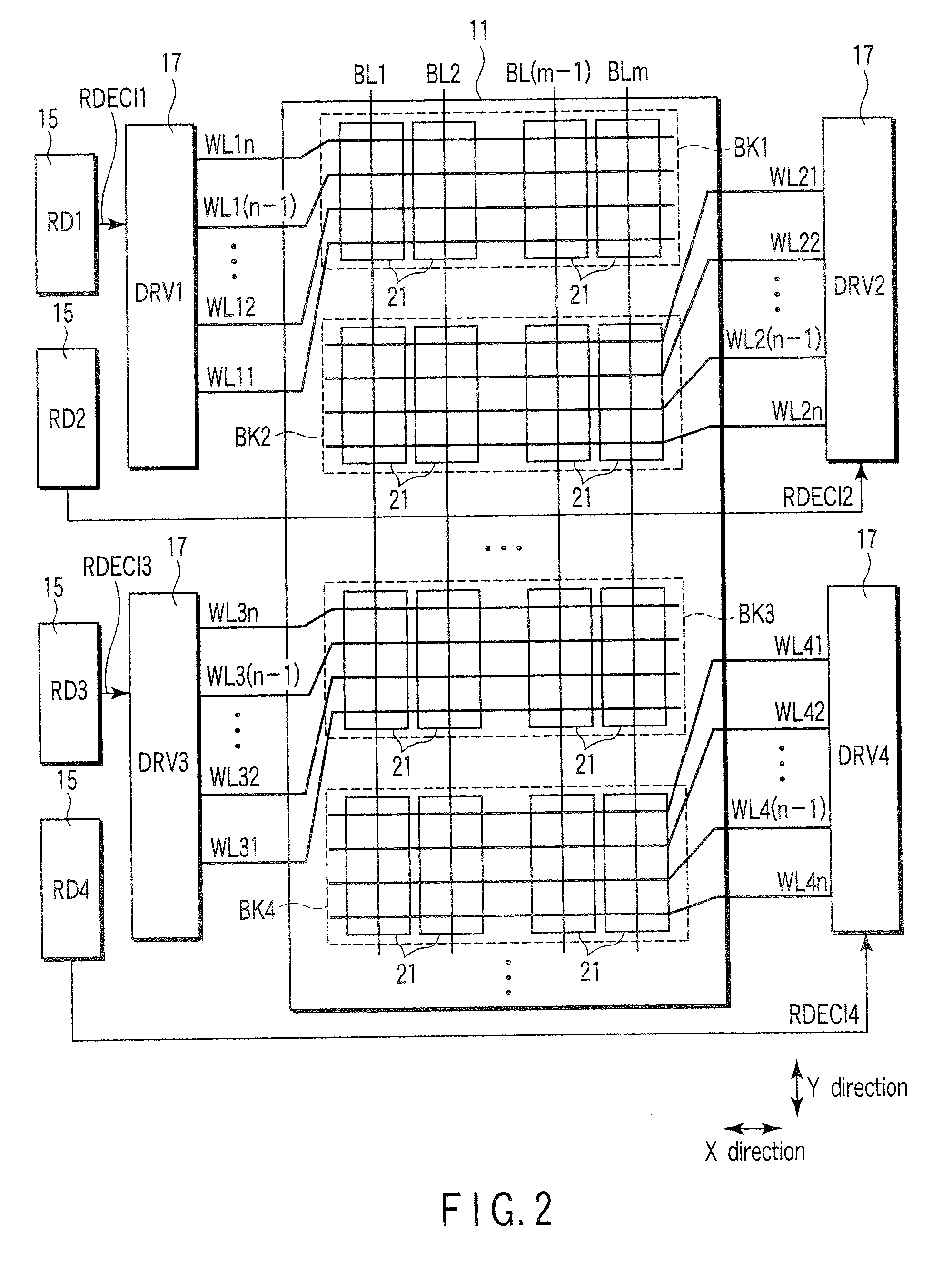
[0041]A memory cell array 11 is composed of blocks B1, BK2, . . . BLj. Each of the blocks BK1, BK2, . . . BLj has a cell unit, and each of the cell units is composed of a NAND string composed of serially connected memory cells, and two select gate transistors connected to both ends thereof one by one.

[0042]A data latch circuit 12 has a function to latch data temporarily at the read / write time, and, for instance, is composed of a flip-flop circuit. An input / output (I / O) buffer 13 functions as an interface circuit of the data, and an address buffer 14 functions as an interface circuit of an address signal.

[0043]A row decoder 15 and a column decoder 16 select a memory cell within the memory cell array 11 based on the address signal. A word line driver 17 drives the selected word line within th...


PUM


Abstract

A semiconductor integrated circuit according to the present invention includes a cell array composed of elements, conductive lines with a pattern of a line & space arranged on the cell array, connecting lines formed upper than the conductive lines, and contact holes which connect the conductive lines to the connecting lines. One end side of the conductive lines sequentially departs from an end of the cell array when heading from one of the conductive lines to another one, the contact holes are arranged at one end side of the conductive lines, and size of the contact holes is larger than width of the conductive lines.

Description

CROSS-REFERENCE TO RELATED APPLICATIONS[0001]This application is based upon and claims the benefit of priority from prior Japanese Patent Application No. 2006-012908, filed Jan. 20, 2006, the entire contents of which are incorporated herein by reference.BACKGROUND OF THE INVENTION[0002]1. Field of the Invention[0003]The present invention relates to a layout of conductive lines having a pattern of a line & space, for instance, which is used for a semiconductor memory with a large memory capacity.[0004]2. Description of the Related Art[0005]In recent years, many electronic apparatuses using a NAND-type flash memory as a main memory have been commercialized. On the other hand, an increase of storage capacity of the NAND-type flash memory becomes a problem as the function of the electronic apparatus increases.[0006]When achieving the increase of the storage capacity, chip layout is very important. For instance, although miniaturization of the memory cell has progressed remarkably, in or...

Claims


Application Information

Patent Timeline
IPC IPC(8): H01L23/52G11C16/04
CPCG11C16/0483G11C16/08H01L27/11529H01L27/105H01L27/11519H01L27/0207H10B41/41H10B41/10H10B41/35H10B63/80
Inventor KATO, YOSHIKOISHIBASHI, SHIGERUNOGUCHI, MITSUHIROHISADA, TOSHIKI
Owner KIOXIA CORP
Why Eureka
Try Eureka