Oscillation circuit

a technology of oscillating circuit and oscillating gate, which is applied in the direction of oscillating generator, pulse technique, pulse generator, etc., can solve the problems of low operation voltage, easy noise, and easy noise in the cycle of output signal q

Inactive Publication Date: 2007-08-09
PANASONIC CORP
View PDF6 Cites 19 Cited by
  • Summary
  • Abstract
  • Description
  • Claims
  • Application Information

AI Technical Summary

Benefits of technology

[0033]In the second oscillation circuit, even when the first voltage fluctuates around the reference voltage due to noise, the number of times the output of the first RS flip flop circuit rises is equal to that counted in the absence of noise. Likewise, even when the second v

Problems solved by technology

In recent years, the semiconductor integrated circuit has experienced process miniaturization to result in low operation voltage, so that errors readily

Method used


Image

  • Oscillation circuit
  • Oscillation circuit
  • Oscillation circuit

Examples


embodiment 1

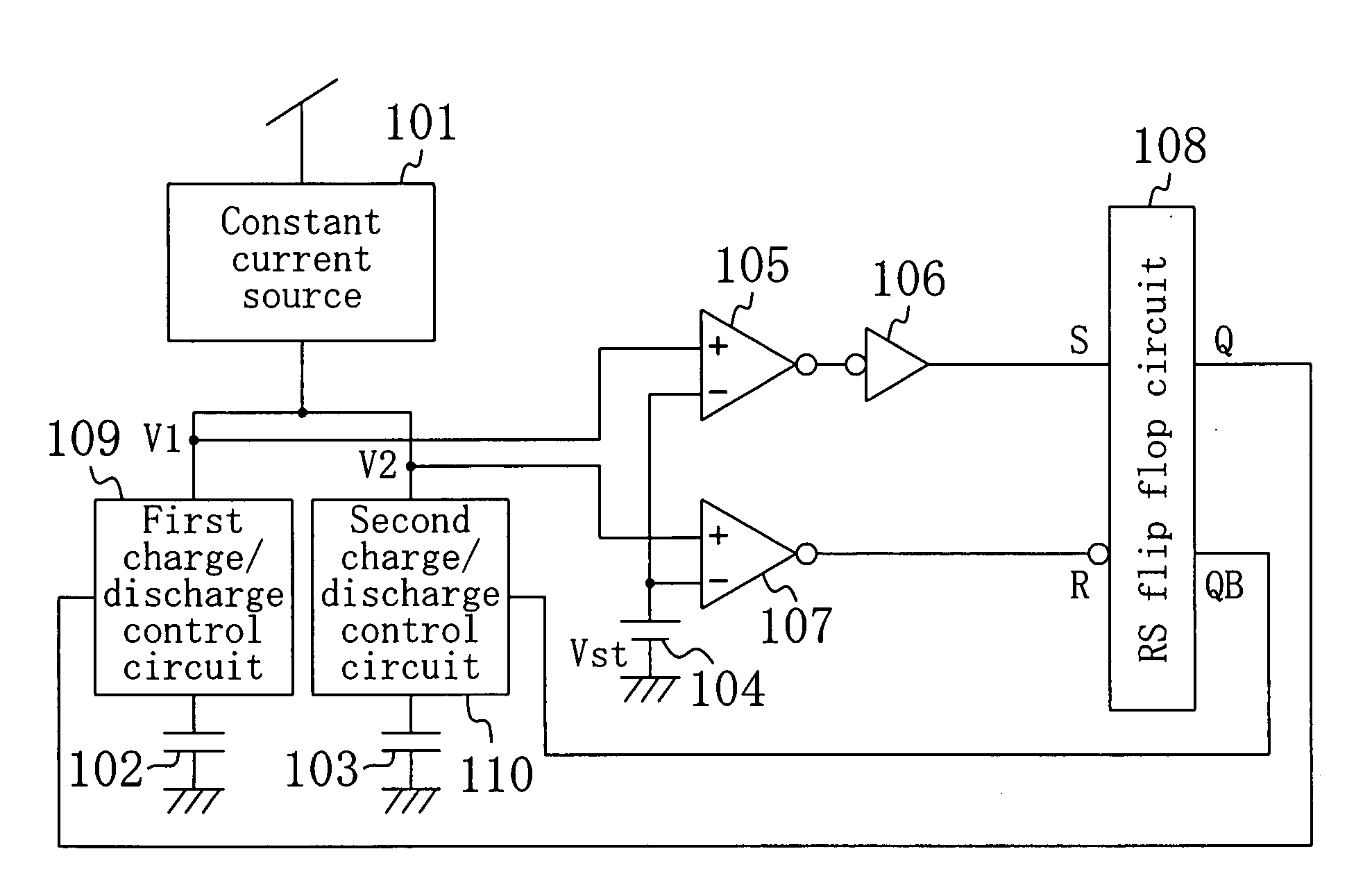
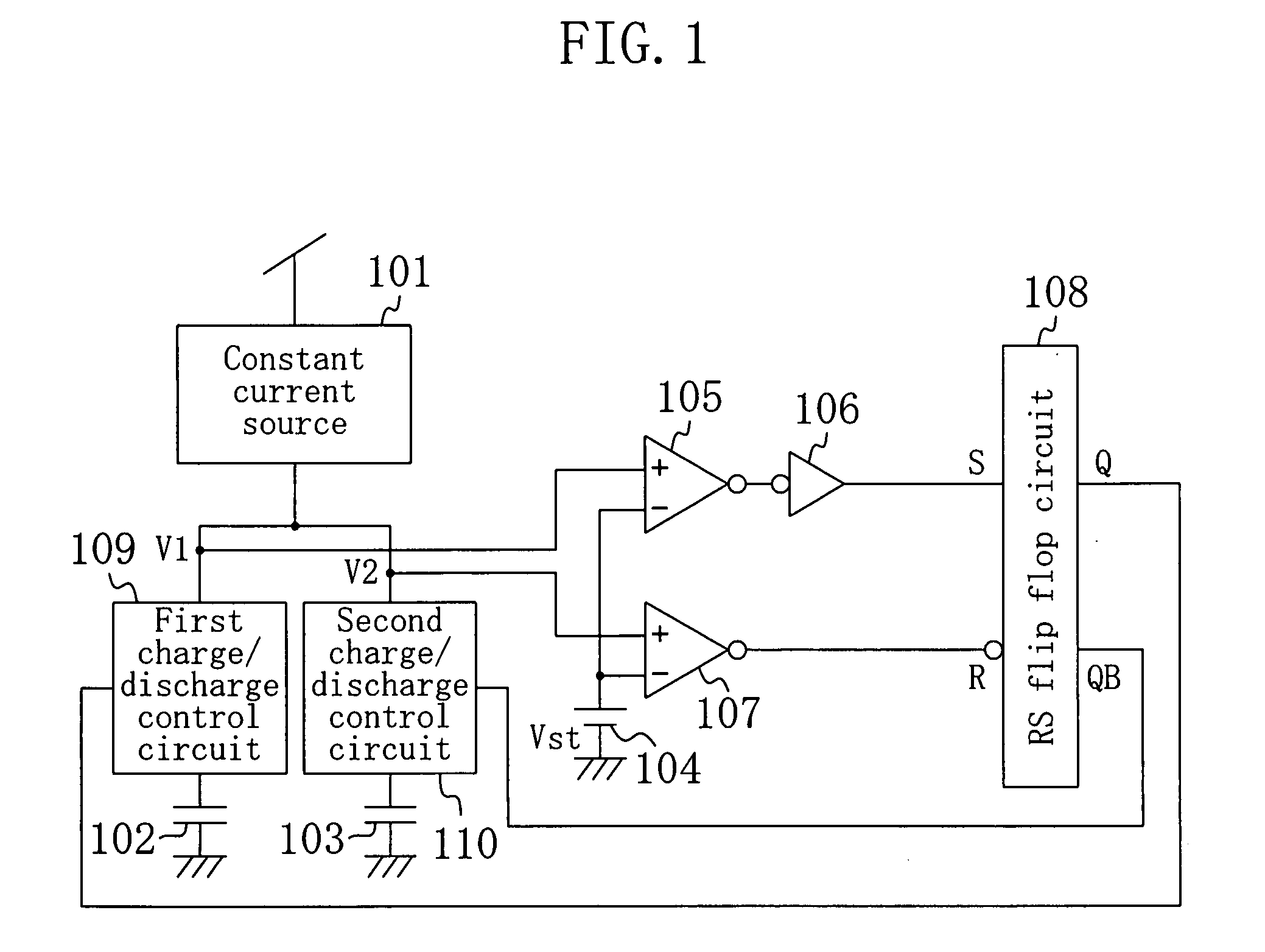
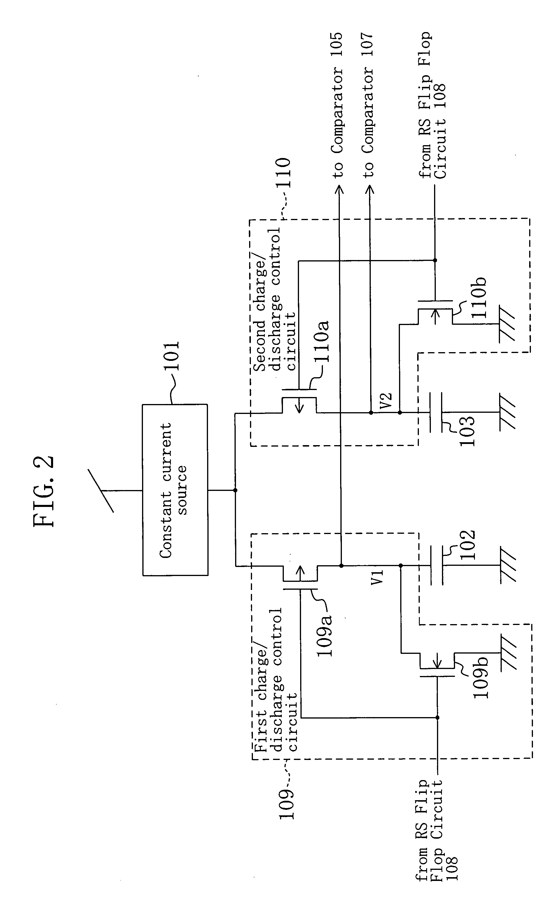
[0079]Referring to FIG. 1, an oscillation circuit of embodiment 1 includes a constant current source 101, a first capacitor 102, a second capacitor 103, a reference power supply 104, a comparator 105, an inverter 106, a comparator 107, an RS flip flop circuit 108, a first charge / discharge control circuit 109, and a second charge / discharge control circuit 110. The oscillation circuit of this embodiment is to be incorporated in a semiconductor integrated circuit.

[0080]The reference power supply 104 generates reference voltage Vst.

[0081]The comparator 105 compares voltage V1, which is determined according to the charge stored in the first capacitor 102, with reference voltage Vst. If voltage V1 is higher, the output of the comparator 105 is at low level. If reference voltage Vst is higher, the output of the comparator 105 is at high level.

[0082]The comparator 107 compares voltage V2, which is determined according to the charge stored in the second capacitor 103, with reference voltage ...

embodiment 2

[0097]Referring to FIG. 4, an oscillation circuit of embodiment 2 includes a constant current source 101, a first capacitor 102, a second capacitor 103, a reference power supply 104, a comparator 105, an inverter 106, a comparator 107, a first charge / discharge control circuit 109, a second charge / discharge control circuit 110, an inverter 201, RS flip flop circuits 202 and 203 (first and second RS flip flop circuits), one-shot circuits 204 and 205 (first and second one-shot circuits), NAND circuits 206 and 207, an OR circuit 208 (logical sum circuit), and a toggle flip flop circuit 209.

[0098]The one-shot circuits 204 and 205 each output a pulse having a predetermined width when the signal input thereto rises. Specifically, as shown in FIG. 5, the one-shot circuits 204 and 205 each include inverters 204a to 204c, NAND circuit 204d, and an inverter 204e. The inverters 204a to 204c delays the signal output from the RS flip flop circuit (202 or 203) by a sufficient amount of delay for t...

embodiment 3

[0112]Referring to FIG. 7, an oscillation circuit of embodiment 3 includes a constant current source 101, a first capacitor 102, a second capacitor 103, a reference power supply 104, a first charge / discharge control circuit 109, a second charge / discharge control circuit 110, comparators 301 and 302 (Schmitt circuits), an NAND circuit 303, and a toggle flip flop circuit 209.

[0113]The comparator 301 (first comparator) outputs a low level signal during a period extending from a time when voltage V1 of the first capacitor 102 is increased by the charging operation to exceed Schmitt voltage Vsc (Schmitt voltage Vsc being defined as a voltage higher than reference voltage Vst by a predetermined width (Schmitt width)) to a time when voltage V1 is decreased to reference voltage Vst by the discharging operation. Other than this period, the comparator 301 outputs a high level signal.

[0114]The comparator 302 (second comparator) outputs a low level signal during a period extending from a time w...


PUM


Abstract

A first comparator outputs a first signal indicative that a voltage determined according to the amount of charge stored in a first capacitor has reached a first reference voltage. A second comparator outputs a second signal indicative that a voltage determined according to the amount of charge stored in a second capacitor has reached a second reference voltage. An RS flip flop circuit is shifted to a set state by one of the first signal and the second signal and shifted to a reset state by the other signal. When the RS flip flop circuit is in the set state, the first capacitor is in a charge state, and the second capacitor is in a discharge state. When the RS flip flop circuit is in the reset state, the first capacitor is in a discharge state, and the second capacitor is in a charge state.

Description

CROSS-REFERENCE TO RELATED APPLICATIONS[0001]This application claims priority under 35 U.S.C. §119(a) on Japanese Patent Application No. 2006-032251 filed on Feb. 9, 2006 and Japanese Patent Application No. 2006-350262 filed on Dec. 26, 2006, the entire contents of which are hereby incorporated by reference.BACKGROUND OF THE INVENTION[0002]1. Field of the Invention[0003]The present invention relates to an oscillation circuit for supplying a signal with stable cycles to a semiconductor integrated circuit, or the like.[0004]2. Description of the Prior Art[0005]In recent years, the semiconductor integrated circuit has experienced process miniaturization to result in low operation voltage, so that errors readily occur due to noise. Thus, a semiconductor integrated circuit (e.g., microcomputer) resistant to noise has been demanded.[0006]A known example of the conventional oscillation circuits is an oscillation circuit for generating a triangular-wave oscillation output using a toggle fli...

Claims


Application Information

Patent Timeline
IPC IPC(8): H03B5/20
CPCH03K4/502H03K3/023H03K3/00
Inventor WAKAI, KATSUSHIYAMANE, ICHIROHAMAGUCHI, TOSHIFUMIRAITA, KAZUHISA
Owner PANASONIC CORP
Why Eureka
Try Eureka