Semiconductor package including transformer or antenna

a technology of semiconductors and transformers, applied in semiconductor devices, semiconductor/solid-state device details, antenna feed intermediates, etc., can solve problems such as obstacles to reducing the overall size of semiconductor packages including antennas and ground shields

Active Publication Date: 2007-08-23
SAMSUNG ELECTRONICS CO LTD
View PDF11 Cites 103 Cited by
  • Summary
  • Abstract
  • Description
  • Claims
  • Application Information

AI Technical Summary

Problems solved by technology

Unfortunately, however, the antenna and the ground shield are generally formed outside semiconductor packages surrounding the semiconductor chips.
Hence, these antennas present an obstacle to reducing the overall size of semiconductor packages including the antenna and the ground shield.

Method used


Image

  • Semiconductor package including transformer or antenna
  • Semiconductor package including transformer or antenna
  • Semiconductor package including transformer or antenna

Examples


Embodiment Construction

[0023]Exemplary embodiments of the invention are described below with reference to the corresponding drawings. These embodiments are presented as teaching examples. The actual scope of the invention is defined by the claims that follow.

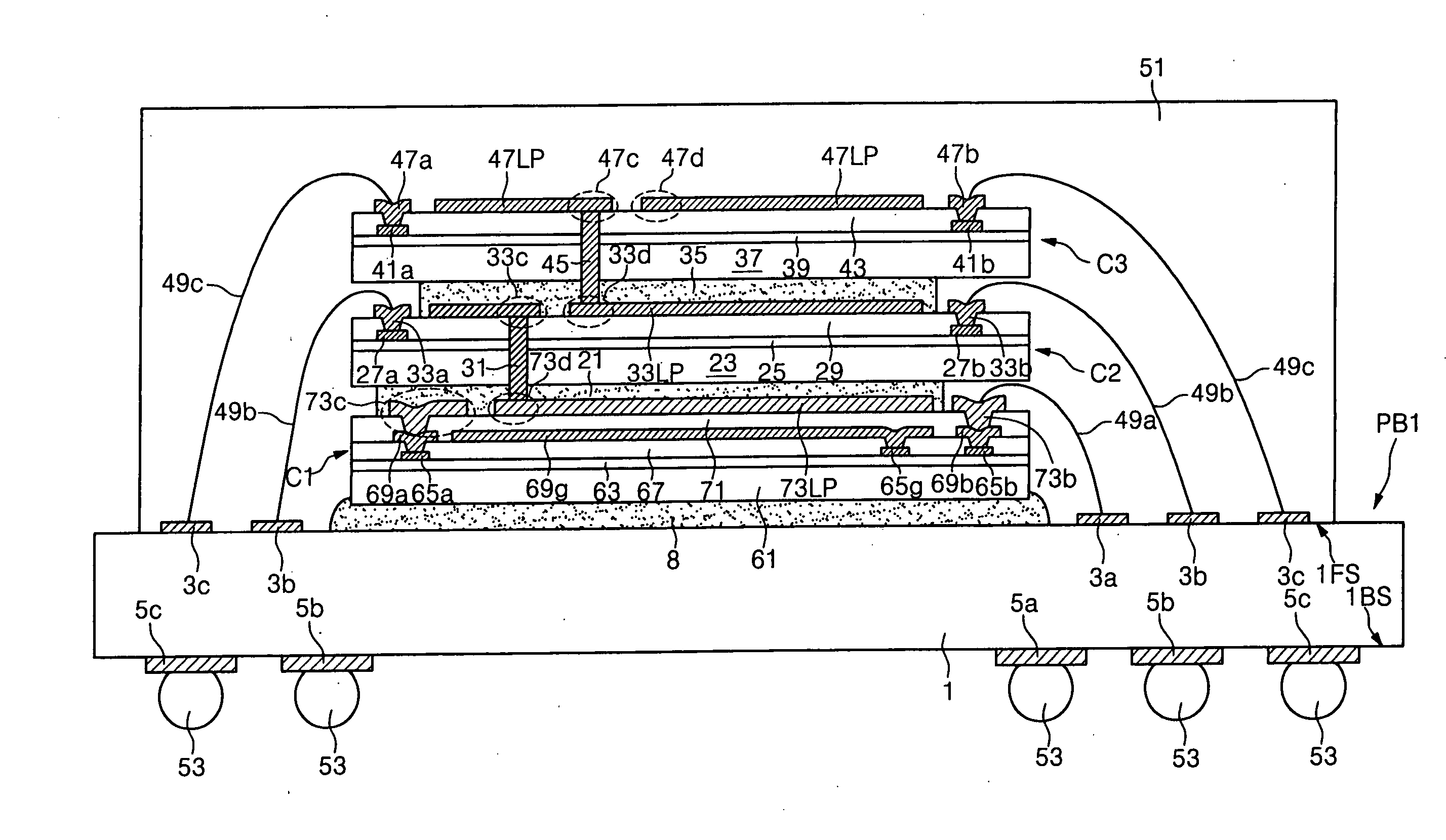
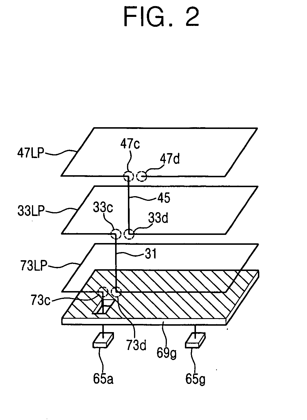
[0024]FIG. 1 is a cross-sectional view of a multi chip package according to one exemplary embodiment of the present invention and FIG. 2 is a perspective view illustrating a helical antenna and a ground shield of the multi chip package shown in FIG. 1.

[0025]Referring to FIGS. 1 and 2, a plurality of semiconductor chips including first through third semiconductor chips C1, C2 and C3, are sequentially stacked on a package board PB1. Package board PB1 comprises a body 1 having a front surface 1FS and a back surface 1BS. Package board PB1 further comprises first through third upper board lines 3a, 3b and 3c formed on front surface 1FS and first through third lower board lines 5a, 5b and 5c formed on back surface 1BS. First through third upper board lines ...


PUM


Abstract

A semiconductor package comprises a package board and a plurality of semiconductor chips sequentially stacked on the package board. Each of the semiconductor chips comprises a semiconductor substrate and an open loop-shaped chip line formed on the semiconductor substrate. The open loop-shaped chip line has first and second end portions. The first and second end portions of the open loop-shaped chip lines are electrically connected to each other by connectors, and the connectors and the open loop-shaped chip lines constitute a spiral antenna.

Description

BACKGROUND OF THE INVENTION[0001]1. Field of the Invention[0002]Embodiments of the invention relate generally to semiconductor packages. More particularly, embodiments of the invention relate to semiconductor packages including a transformer or an antenna.[0003]A claim of priority is made to Korean Patent Application No. 2006-17903, filed Feb. 23, 2006, the disclosure of which is hereby incorporated by reference in its entirety.[0004]2. Description of Related Art[0005]As the size of portable electronic devices continues to shrink, the size of semiconductor packages mounted in the portable electronic devices must be scaled down accordingly. In addition, to increase the computational and / or memory capacity of circuits within the semiconductor packages, packaging techniques have been developed for mounting a plurality of semiconductor chips in a single semiconductor package. These packaging techniques include, for example, a multi chip package (MCP) technique, a multi-stack package (MS...

Claims


Application Information

Patent Timeline
Patent Type & Authority Applications(United States)
IPC IPC(8): H01L23/02
CPCH01L23/3121H01L23/3128H01L2224/73265H01L2224/73253H01L2224/73204H01L2224/16225H01L2924/01074H01L2924/01006H01L24/48H01Q9/27H01L2924/3025H01L2924/30107H01L2924/15311H01L2924/1423H01L2924/01082H01L2924/01078H01L2924/01033H01L2924/01013H01L2225/06586H01L2225/06541H01L2225/06527H01L2225/06524H01L2225/06513H01L2225/0651H01L2224/48227H01L2224/48091H01L2224/32225H01L2224/32145H01L2224/16145H01L23/5227H01L24/73H01L25/0657H01L2924/00014H01L2924/00H01L2224/451H01L2924/181H01L24/45H01L2924/14H01L2224/05001H01L2224/73257H01L24/05H01L2224/45099H01L2224/05599H01L2924/00012H01L23/12
Inventor CHOI, YUN-SEOKLEE, HEE-SEOK
Owner SAMSUNG ELECTRONICS CO LTD
Why Eureka
Try Eureka