Display device
a display device and display screen technology, applied in the field of display devices, can solve the problems of poor image quality due to dust that cannot be satisfactorily suppressed, damage to the lc panel unit b>12/b>, etc., and achieve the effect of suppressing the generation of dust and excellent image quality
- Summary
- Abstract
- Description
- Claims
- Application Information
AI Technical Summary
Benefits of technology
Problems solved by technology
Method used
Image

Examples
first embodiment
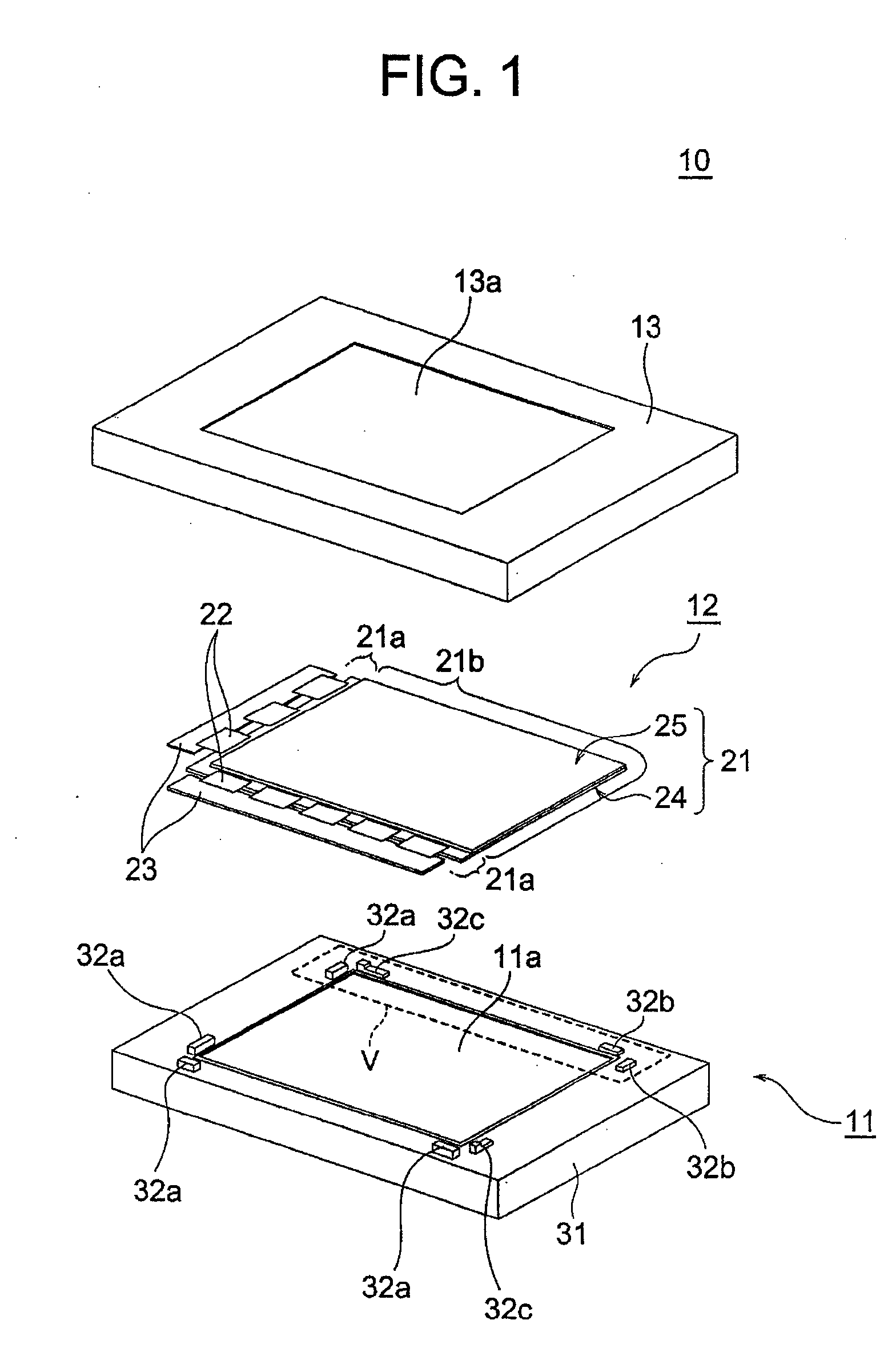
[0059]FIG. 1 is an exploded perspective view of a LCD device according to the present invention. The LCD device, generally designated at numeral 10, has a configuration similar to that of the conventional LCD device 100 shown in FIGS. 17 to 19 except for the shape of the positioning ribs formed on the backlight unit 11.
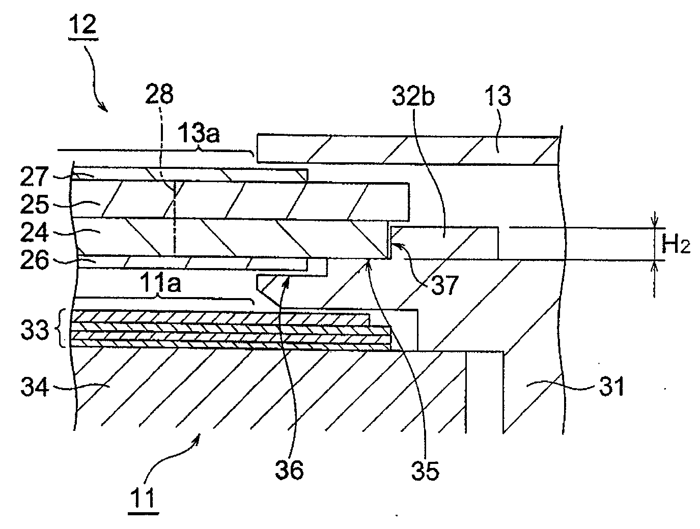
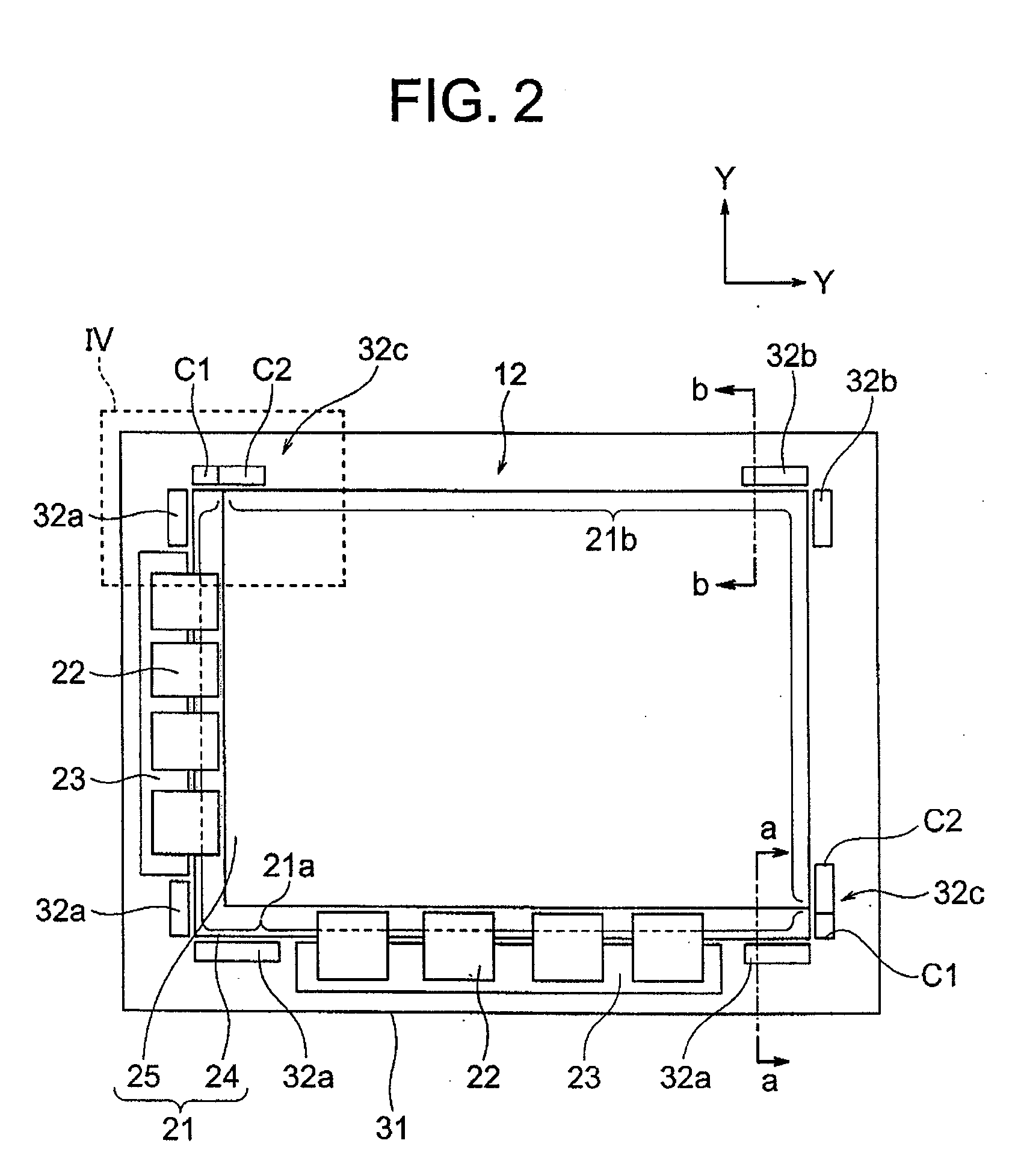
[0060]In the display panel 21, the TFT substrate 24 shown as the bottom side of the display panel unit 12 has an edge protruding from the edge of the counter substrate 25 shown as the top side of the display panel unit 12, on two adjacent sides of the rectangular display panel 21 to which TCPs 22 are connected. The TFT substrate 24 has an edge aligned with the edge of the counter substrate on the remaining two adjacent sides of the display unit 12. In other words, the edge of the display panel 21 includes a first edge portion 21a in which the edge of the TFT substrate 24 protrudes from the corresponding edge of the counter substrate 25, and a second edge portion 21b i...
second embodiment
[0080]FIG. 13A is a perspective view showing, similarly to FIG. 5, the configuration of a LCD device according to the present invention. FIG. 13B is a sectional view taken along line b-b shown in FIG. 13A. In the LCD device generally designated at numeral 70, the second type rib 32b has a positioning wall 71 opposing the edge surface of the counter substrate 25, and a retracted wall 72 formed between the bottom of the second type rib 32b and the positioning wall 71. The retracted wall 72 is formed at a position retracted from the positioning wall 71 with respect to the display panel 21.
[0081]The distance between the surface of the positioning wall 71 and the surface of the retracted wall 72, as observed normal to the display panel 21, is set sufficiently larger than the range of misalignment estimated between the edge surface of the TFT substrate 24 and the edge surface of the counter substrate 25. The second type positioning ribs 32b are formed only in a portion opposing the second...
third embodiment
[0083]FIG. 23A shows in a perspective view, similarly to FIG. 5, a LCD device according to the present invention, and FIG. 23B shows a sectional view taken along line b-b in FIG. 23B. The LCD device, generally designated at numeral 74, is similar to the LCD device 10 shown in FIG. 5 except that the second type positioning ribs 32b in the present embodiment include a second positioning wall 71 opposing the second outer edge portion 21b of the display panel 21 and a groove 75 formed on the second positioning wall 71 at the height where the bonding surface of the display panel 21 and the second positioning wall 71 intersect. One of the second type positioning ribs 32b positioned adjacent to the first type positioning ribs 32a opposes only the second outer edge portion 21b of the display panel 21. The bottom of the groove 75 configures a retracted wall of the second type positioning ribs 32b in the present embodiment.
[0084]The height of the center of the groove 75 with respect to the mo...
PUM
| Property | Measurement | Unit |
|---|---|---|
| distance | aaaaa | aaaaa |
| height | aaaaa | aaaaa |
| thickness | aaaaa | aaaaa |
Abstract
Description
Claims
Application Information
 - R&D
- Intellectual Property
- Life Sciences
- Materials
- Tech Scout
- Unparalleled Data Quality
- Higher Quality Content
- 60% Fewer Hallucinations
Browse by: Latest US Patents, China's latest patents, Technical Efficacy Thesaurus, Application Domain, Technology Topic, Popular Technical Reports.
© 2025 PatSnap. All rights reserved.Legal|Privacy policy|Modern Slavery Act Transparency Statement|Sitemap|About US| Contact US: help@patsnap.com