Liquid crystal display device and method for driving the same

a liquid crystal display and display device technology, applied in static indicating devices, non-linear optics, instruments, etc., can solve the problems of insufficient time to fully charge a data voltage into the pixels, insufficient data charging time, and limitation in increasing the tft siz

Inactive Publication Date: 2007-11-22
LG DISPLAY CO LTD
View PDF36 Cites 14 Cited by
  • Summary
  • Abstract
  • Description
  • Claims
  • Application Information

AI Technical Summary

Benefits of technology

[0030]An advantage of the present invention is to provide a liquid crystal display device and a method for driving the same which are capable of supplying a scan pulse from one gate line to vertically-adjacent pixels, and thus, securing a sufficient data charging time even when one frame is driven under the condition in which the frame is divided into a plurality of sub-frames.
[0031]Additional features and advantages of the invention will be set forth in the description which follows, and in part will be apparent from the description, or may be learned from practice of the invention. The objectives and other advantages of the invention will be realized and attained by the structure particularly pointed out in the written description and claims hereof as well as the appended drawings.
[0032]To achieve these and other advantages and in accordance with the purpose of the invention, as embodied and broadly described herein, a liquid crystal display device includes a plurality of gate lines; a plurality of data lines that cross the gate lines to define pixel regions; a plurality of thin film transistors at the crossings of the gate and data lines, the thin film transistors of vertically adjacent pixels each connected to a shared gate line of the plurality of gate lines and on opposite sides of the shared gate line; and a plurality of pixel electrodes in the pixel regions, wherein each pixel electrode of the plurality of pixel electrodes is formed in two horizontally-adjacent pixel regions.
[0033

Problems solved by technology

The color filter layers add significantly to the manufacturing costs for a liquid crystal display device.
As a result, for large sized LCD devices, there may be insufficient time to completely charge a data voltage into the pixels.
Al

Method used


Image

  • Liquid crystal display device and method for driving the same
  • Liquid crystal display device and method for driving the same
  • Liquid crystal display device and method for driving the same

Examples


first embodiment

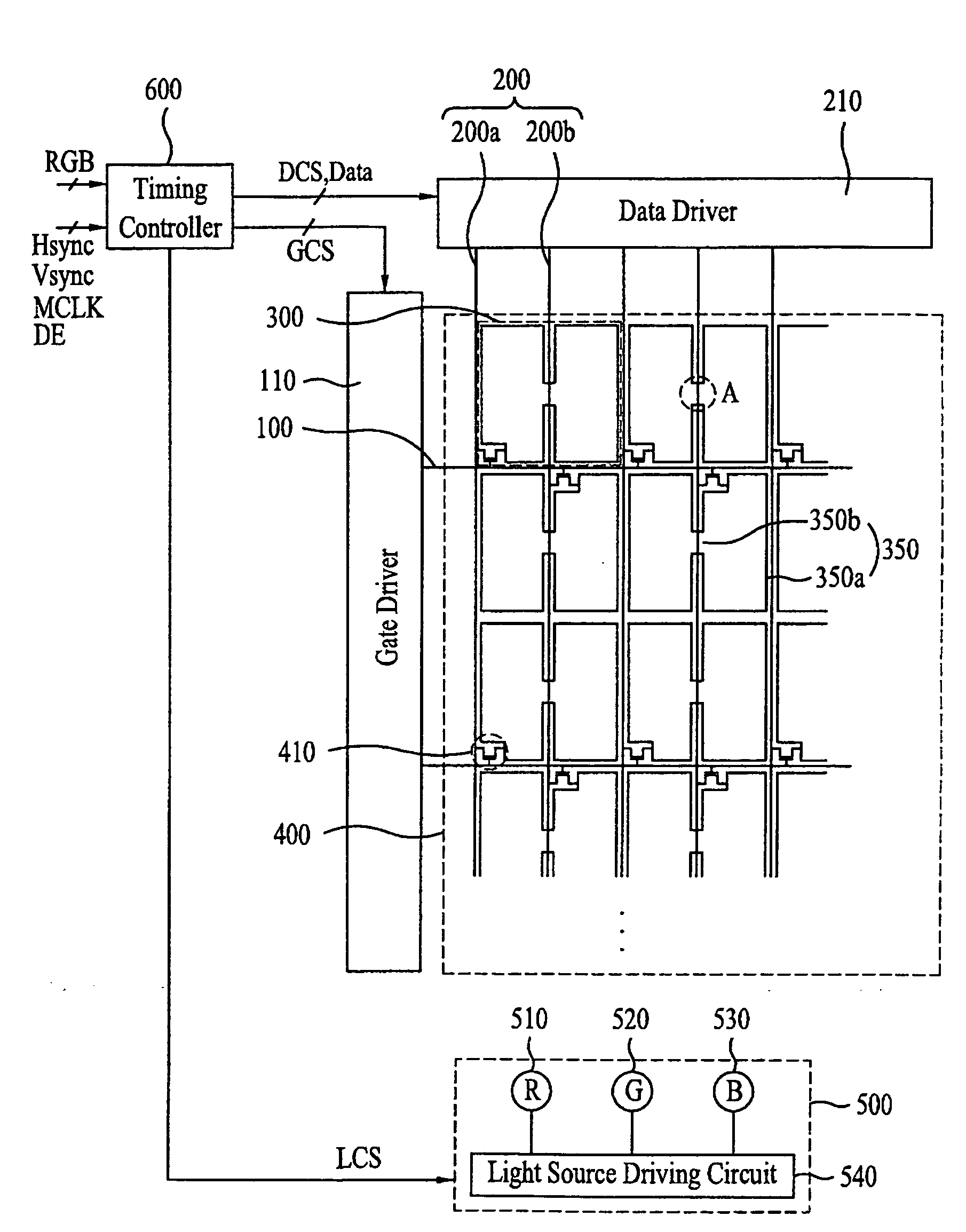
[0043]FIG. 3 is a plan view schematically illustrating a liquid crystal display (LCD) device according to the present invention.

[0044]As shown in FIG. 3, the LCD device according to the first embodiment of the present invention includes a liquid crystal panel 400 including a plurality of gate lines 100 and a plurality of data lines 200 crossing the gate lines 100 to define pixel regions, wherein one pixel 300 is formed to include two horizontally-adjacent pixel regions, and a backlight unit 500 for sequentially irradiating red (R), green (G), and blue (B) lights to the liquid crystal panel 400. The LCD device also includes a data driver 210 for dividing one frame into a plurality of sub-frames and supplying data to the data lines 200 of the liquid crystal panel 400 for every sub-frame, a gate driver 110 for supplying scan pulses to the gate lines 100 of the liquid crystal panel 400, and a timing controller 600 for controlling the gate driver 110, data driver 210, and backlight unit ...

second embodiment

[0065]FIG. 4 is a plan view schematically illustrating an LCD device according to the present invention.

[0066]Referring to FIG. 4, the LCD device according to the second embodiment of the present invention is similar to the LCD device according to the first embodiment, except for the number of data lines 200 and the structure of the liquid crystal panel 400.

[0067]In the LCD device according to the second embodiment of the present invention, the liquid crystal panel 400 is configured such that one pixel 300 includes four horizontally-adjacent pixel regions, and a plurality of thin film transistors (TFTs) 410 formed at the crossings of odd gate lines 100 and (4n−3)th and (4n−2)th data lines 200 and the crossings of even gate lines 100 and (4n−1)th and (4n)th data lines 200, where n is a natural number. The TFTs 410 are arranged at opposite sides of the gate line 100 in a zigzag arrangement along with the gate line 100. Two pixels 300 are vertically arranged between the adjacent two ga...


PUM


Abstract

A liquid crystal display (LCD) device includes: a plurality of gate lines; a plurality of data lines that cross the gate lines to define pixel regions; a plurality of thin film transistors at the crossings of the gate and data lines, the thin film transistors of vertically adjacent pixels each connected to a shared gate line of the plurality of gate lines and on opposite sides of the shared gate line; and a plurality of pixel electrodes in the pixel regions, wherein each pixel electrode of the plurality of pixel electrodes is formed in two horizontally-adjacent pixel regions.

Description

[0001]This application claims the benefit of Korean Patent Application No. 10-2006-0045641, filed on May 22, 2006, which is hereby incorporated by reference for all purposes as if fully set forth herein.BACKGROUND OF THE INVENTION[0002]1. Field of the Invention[0003]The present invention relates to a liquid crystal display (LCD) device and more particularly to an LCD device and a method for driving the same.[0004]2. Discussion of the Related Art[0005]Among various ultra-thin flat type display devices, which include devices having a display screen thickness several centimeters or less, liquid crystal display (LCD) devices are widely used for notebook computers, monitors, and spacecraft and aircraft displays because or their advantages such as low operating voltage, low power consumption, and portability.[0006]A typical LCD device includes a lower substrate, an upper substrate, and a liquid crystal layer formed between the substrates.[0007]Gate lines and data lines substantially perpe...

Claims


Application Information

Patent Timeline
IPC IPC(8): G09G3/36
CPCG09G3/3648G09G2300/0426G09G2310/0235G09G2310/0205G09G2300/0443G02F1/133
Inventor KANG, BYUNG KOOKIM, EUI TAE
Owner LG DISPLAY CO LTD
Why Eureka
Try Eureka