LCD Panel and LCD Device

a technology of liquid crystal display and lcd device, which is applied in the field of lcd panel, can solve the problems of degradation of the experience of the user who uses the lcd device, insufficient and short charging time available for each of the gates, so as to reduce the number of scanning times, prolong the charging time of the gates of tfts, and high frame rate

Active Publication Date: 2013-05-23
TCL CHINA STAR OPTOELECTRONICS TECH CO LTD
View PDF3 Cites 5 Cited by
  • Summary
  • Abstract
  • Description
  • Claims
  • Application Information

AI Technical Summary

Benefits of technology

[0026]The present disclosure has the following benefits as compared to the prior art: when two adjacent charging scanning lines are being scanned in the LCD panel of the present disclosure, two adjacent discharging scanning lines connected the pixel units in other rows different from those of the two adjacent charging scanning lines being scanned are also scanned within a same scanning time frame. As compared to the prior art where only one scanning line is scanned within one scanning period, the present disclosure can extend the charging time of gates of TFTs by reducing the number of times of scanning; and furthermore, the LCD panel can operate at a high frame rate to improve the experience of the user who uses the LCD panel and the LCD device.

Problems solved by technology

Due to a large number of gates in the high-fineness LCD device, the charging time available for each of the gates becomes relatively short.
If the high-fineness LCD device is further demanded for a higher frame rate, the charging time of the gates is seriously insufficient.
This will cause degradation in experience of the user who uses the LCD device.

Method used


Image

  • LCD Panel and LCD Device
  • LCD Panel and LCD Device
  • LCD Panel and LCD Device

Examples


first embodiment

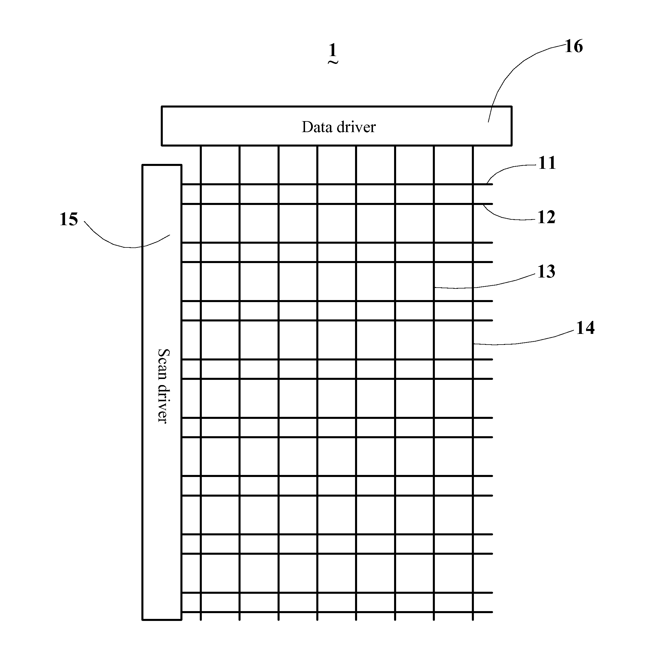
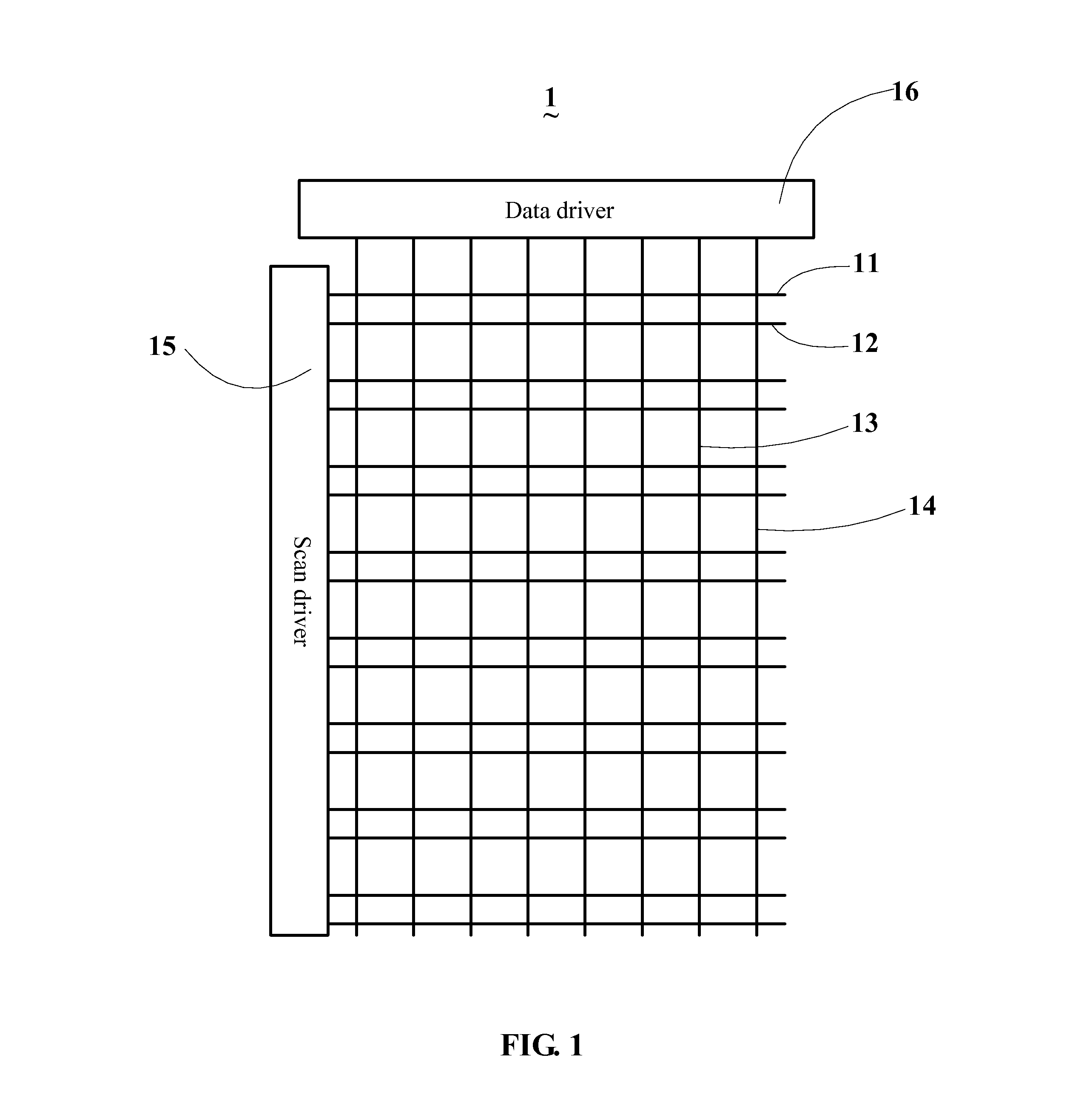
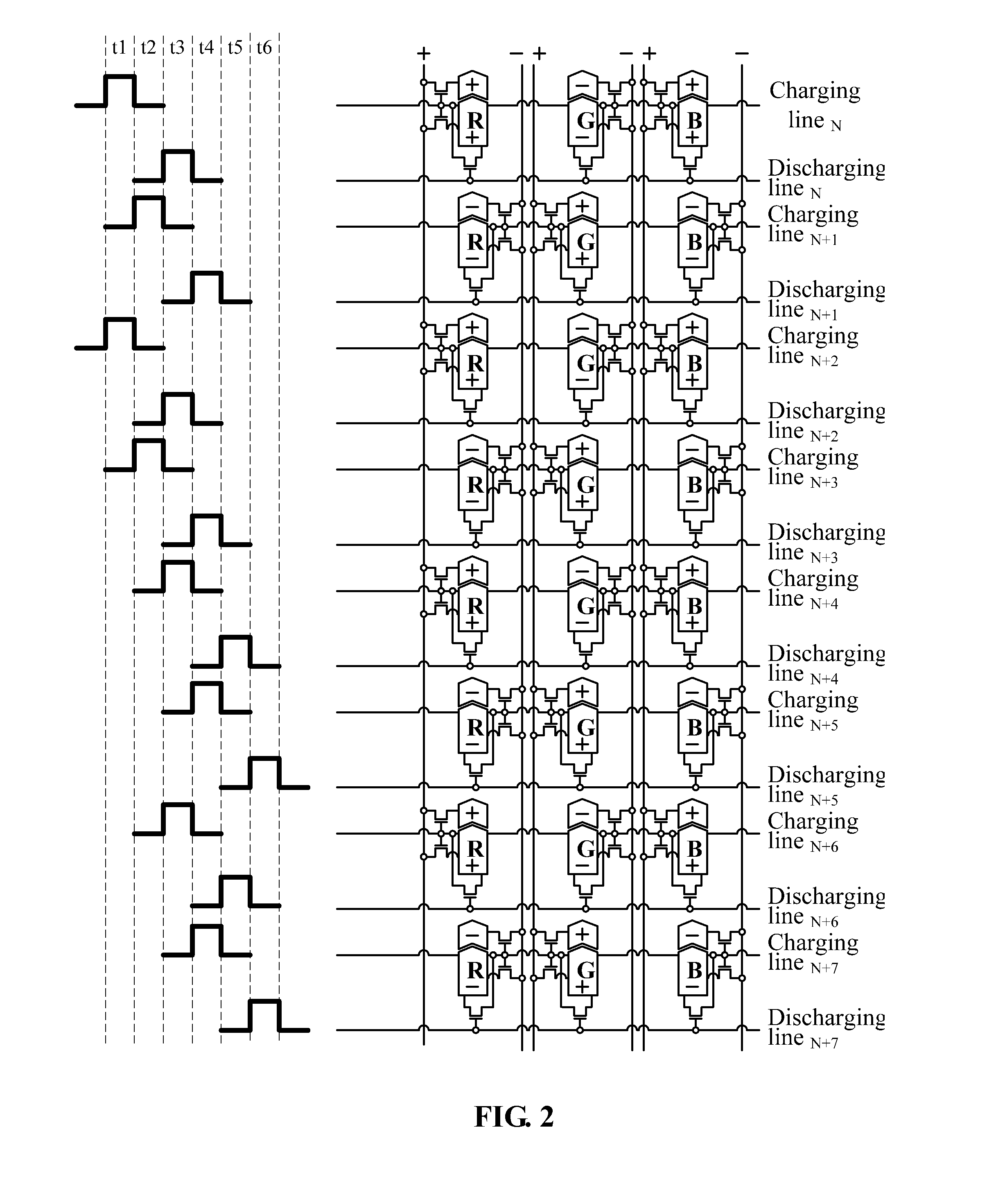
[0040]FIG. 2 is a schematic view illustrating electrode structures of the LCD panel and a scanning signal timing sequence thereof according to the present disclosure. Referring to FIG. 2, the charging scanning lines 11 are represented as a charging scanning line N to a charging scanning line N+7, and the discharging scanning lines 12 are represented as a discharging scanning line N to a discharging scanning line N+7. A charging scanning line and a discharging scanning line that have a same reference numeral are electrically connected to pixel units in a same row; e.g., the charging scanning line N and the discharging scanning line N are electrically connected to pixel units in an Nth row. In addition, t1 to t6 represent scanning time frames in a time sequence.

[0041]As shown in FIG. 2, within the scanning time frame t1, a scanning pulse signal of a high level is inputted by the scan driver 15 into the charging scanning line N and the charging scanning line N+2 simultaneously. Then, t...

second embodiment

[0054]FIG. 3 is a schematic view illustrating electrode structures of the LCD panel and a scanning signal timing sequence thereof according to the present disclosure. As shown in FIG. 3, the charging scanning lines 11 are represented as a charging scanning line N to a charging scanning line N+7, and the discharging scanning lines 12 are represented as a discharging scanning line N to a discharging scanning line N+7. A charging scanning line and a discharging scanning line that have a same reference numeral are electrically connected to pixel units in a same row; e.g., the charging scanning line N and the discharging scanning line N are electrically connected to pixel units in an Nth row. In addition, t1 to t13 represent scanning time frames in a time sequence.

[0055]As shown in FIG. 3, within the scanning time frame t1, a scanning pulse signal of a high level is inputted by the scan driver 15 into the charging scanning line N, the charging scanning line N+1, the charging scanning lin...


PUM


Abstract

A liquid crystal display (LCD) device and an LCD panel are disclosed. The LCD panel comprises charging scanning lines, discharging scanning lines, first data lines, second data lines and pixel units. The charging scanning lines and the discharging scanning lines are arranged alternately and parallel with each other in a first direction. The first data lines and the second data lines are arranged parallel with each other in a second direction and insulatedly intersect the charging scanning lines and the discharging scanning lines. Each pixel unit comprises a charging TFT, a discharging TFT and a pixel electrode. When two adjacent charging scanning lines are being scanned in the LCD panel, two adjacent discharging scanning lines located in other rows different from those of the two adjacent charging scanning lines being scanned are scanned within a same scanning time frame. The LCD panel can extend the charging time of gates.

Description

FIELD OF THE INVENTION[0001]The present disclosure generally relates to a liquid crystal display (LCD) panel, and more particularly, to an LCD panel adapted to operate at a high frame rate; and the present disclosure also relates to an LCD device comprising the LCD panel.BACKGROUND OF THE INVENTION[0002]An LCD has advantages of portability, low power consumption, and low radiation. Therefore, the LCD has been widely used in various information products such as TV sets, notebooks, computers, mobile phones and personal digital assistants (PDAs).[0003]In a high-fineness LCD device, when the scanning lines are applied scanning signals, the gates connected to the scanning lines may be charged. Due to a large number of gates in the high-fineness LCD device, the charging time available for each of the gates becomes relatively short. If the high-fineness LCD device is further demanded for a higher frame rate, the charging time of the gates is seriously insufficient. This will cause degradat...

Claims


Application Information

Patent Timeline
Patent Type & Authority Applications(United States)
IPC IPC(8): G06T15/00G09G5/00
CPCG09G3/3266G09G2330/021G09G2320/0252G09G3/3674
Inventor HOU, HUNG-LUNGLEE, CHIA-YUHE, CHENGMING
Owner TCL CHINA STAR OPTOELECTRONICS TECH CO LTD
Why Eureka
Try Eureka