Eureka AIR delivers breakthrough ideas for toughest innovation challenges, trusted by R&D personnel around the world.

Semiconductor memory device having stacked gate including charge accumulation layer and control gate and test method thereof

Inactive Publication Date: 2007-12-27
TOSHIBA MEMORY CORP
View PDF4 Cites 4 Cited by
  • Summary
  • Abstract
  • Description
  • Claims
  • Application Information

AI Technical Summary

Benefits of technology

[0008] a memory cell which has a first MOS transistor including a charge accumulation layer and a control gate formed on the charge accumulation layer;
[0009]

Problems solved by technology

However, with the configuration disclosed in the above Publication, there occurs a problem that the potential of a bit line is lowered if a failure in which another bit line is shorted to ground potential occurs, for example.

Method used


Image

  • Semiconductor memory device having stacked gate including charge accumulation layer and control gate and test method thereof
  • Semiconductor memory device having stacked gate including charge accumulation layer and control gate and test method thereof
  • Semiconductor memory device having stacked gate including charge accumulation layer and control gate and test method thereof

Examples


Embodiment Construction

[0029] There will now be described an embodiment of this invention with reference to the accompanying drawings. In the following explanation, the state in which charges are stored in the charge accumulation layer is defined as a “program state” and the state in which charges are extracted is defined as an “erase state”.

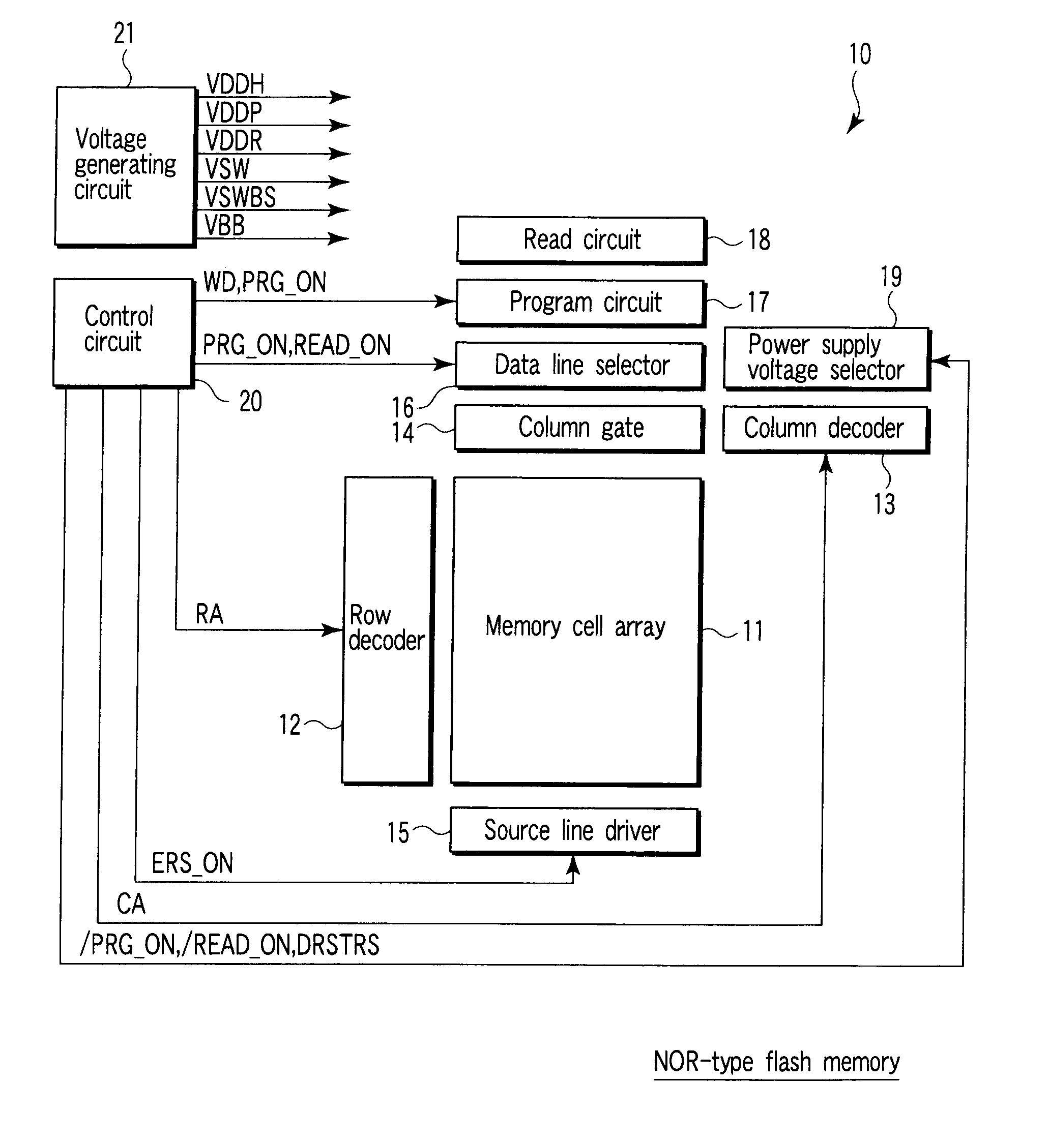
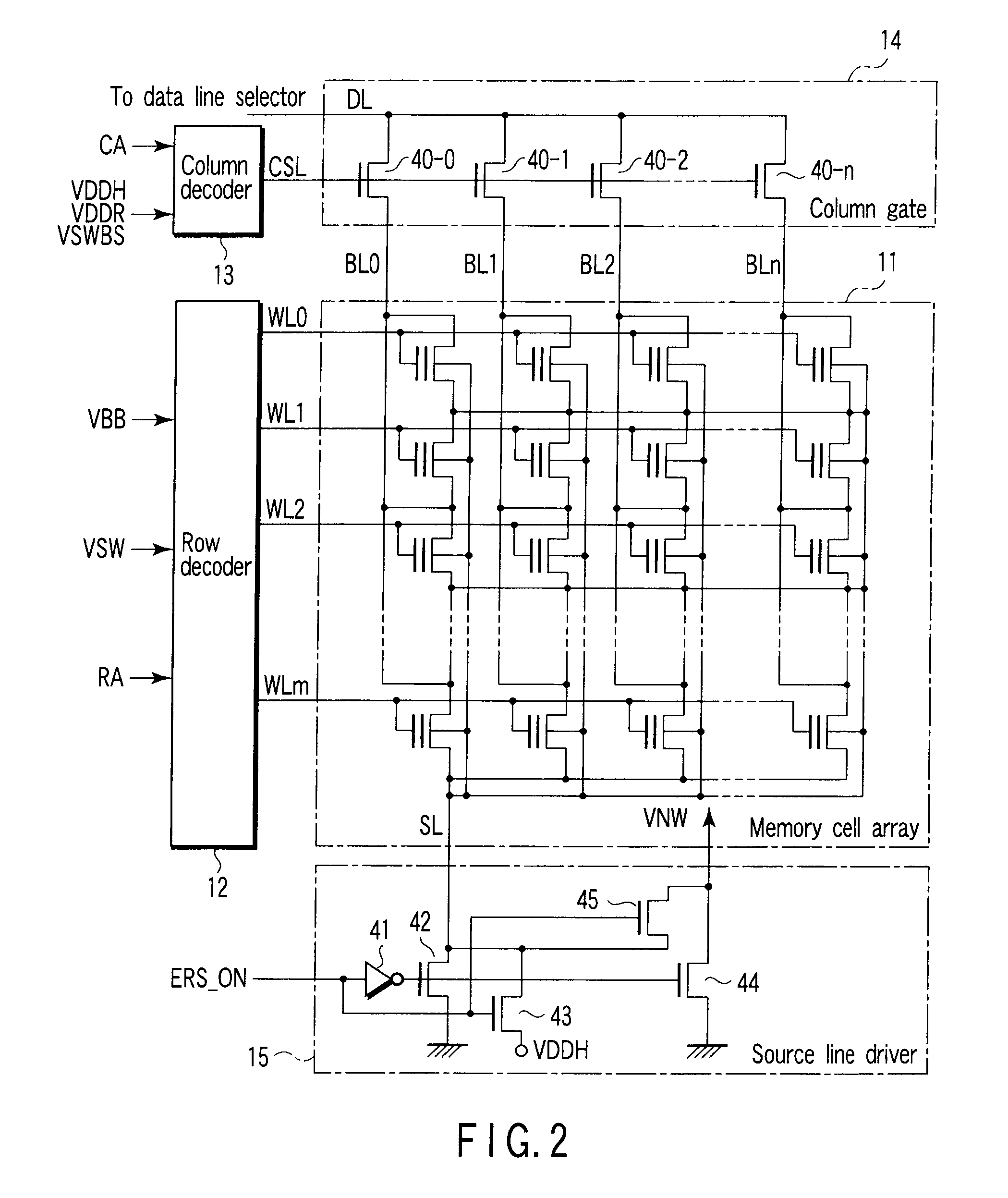
[0030] A semiconductor memory device and a test method thereof according to one embodiment of this invention are explained below. FIG. 1 is a block diagram of a NOR flash memory according to the present embodiment. As shown in FIG. 1, a flash memory 10 includes a memory cell array 11, row decoder 12, column decoder 13, column gate 14, source line driver 15, data line selector 16, program circuit 17, read circuit 18, power supply voltage selector 19, control circuit 20 and voltage generating circuit 21.

[0031] The memory cell array 11 has a plurality of NOR flash memory cells arranged in a matrix form. The memory cells are connected to bit lines, word lines and a sour...


PUM


Abstract

A semiconductor memory device includes a memory cell, a word line, a bit line, a column gate, and a power supply decode circuit. The memory cell has a first MOS transistor including a charge accumulation layer and a control gate. The bit line is connected to a drain of the first MOS transistor and is applied with first voltage at the test operation time and at data program operation time. The column gate includes a second MOS transistor having current path connected to the bit line to transfer the first voltage to the bit line at the test operation time. The power supply decode circuit applies a second voltage to a gate of the second MOS transistor at the program operation time and applies a third voltage lower than the second voltage at the test operation time.

Description

CROSS-REFERENCE TO RELATED APPLICATIONS [0001] This application is based upon and claims the benefit of priority from prior Japanese Patent Application No. 2006-171856, filed Jun. 21, 2006, the entire contents of which are incorporated herein by reference. BACKGROUND OF THE INVENTION [0002] 1. Field of the Invention [0003] This invention relates to a semiconductor memory device and a test method thereof and, for example, to a semiconductor memory having stacked gate including charge accumulation layer and control gate. [0004] 2. Description of the Related Art [0005] Conventionally, a NOR flash memory is known as an electrically data rewritable nonvolatile semiconductor memory. In the NOR flash memory, a drain stress test is made before shipment in order to attain the high reliability of the operation thereof. The drain stress test is to apply voltage to the drain of the memory cell and check whether a leakage of charges occurs or not. [0006] Conventionally, a method of applying prog...

Claims


Application Information

Patent Timeline
IPC IPC(8): G11C5/14
CPCG11C16/04G11C29/12005G11C29/12
Inventor HARA, TOKUMASA
Owner TOSHIBA MEMORY CORP
Why Eureka
Eureka Blog
Learn More