Light-emitting element, light-emitting device, and electronic device

a technology of light-emitting elements and electronic devices, which is applied in the direction of solid-state devices, semiconductor lamps, thermoelectric devices, etc., can solve the problems of difficult to obtain character, short life of elements, and inability to obtain light-emitting with good color purity, and achieve superior color purity and good color purity

Active Publication Date: 2008-01-10
SEMICON ENERGY LAB CO LTD
View PDF7 Cites 81 Cited by
  • Summary
  • Abstract
  • Description
  • Claims
  • Application Information

AI Technical Summary

Benefits of technology

[0013]Accordingly, it is an object of the present invention to provide a long-life light-emitting element which is superior in color purity, in a case where an organic compound is used for a substance with a light-emitting property. It is another object to provide a long-life light-emitting device and electronic device which are superior in color purity.
[0024]In the light-emitting element of the present invention, a light-emitting region is formed not at an interface between a light-emitting layer and a hole transporting layer or an interface between a light-emitting layer and an electron transporting layer but in the vicinity of the center of the light-emitting layer. Further, a long-life light-emitting element in which an element is not easily deteriorated can be obtained. Also in a case where a hole transporting layer and an electron transporting layer do not exist, the similar effect can be obtained by providing a light-emitting region not at an interface between both electrodes and a light-emitting layer but in the vicinity of the center of the light-emitting layer.
[0025]Further, in the light-emitting element of the present invention, emission color of the first organic compound and emission color of the third organic compound are similar colors. Accordingly, light emission with good color purity can be obtained even when not only the first organic compound but also the third organic compound emits light.
[0026]Furthermore, by application of the light-emitting element of the present invention to a light-emitting device and an electronic device, a long-life light-emitting device and electronic device which are superior in color purity can be obtained.

Problems solved by technology

This characteristic is difficult to be obtained by a point light source typified by an incandescent lamp or an LED, or a line light source typified by a fluorescent lamp.
However, in Patent Document 1, since doping with plural kinds of fluorescent substances having different colors is performed, light emission with good color purity cannot be obtained, even though white light emission with good color stability can be obtained.
However, there is a problem that the element has the short life.

Method used


Image

  • Light-emitting element, light-emitting device, and electronic device
  • Light-emitting element, light-emitting device, and electronic device
  • Light-emitting element, light-emitting device, and electronic device

Examples


embodiment mode 1

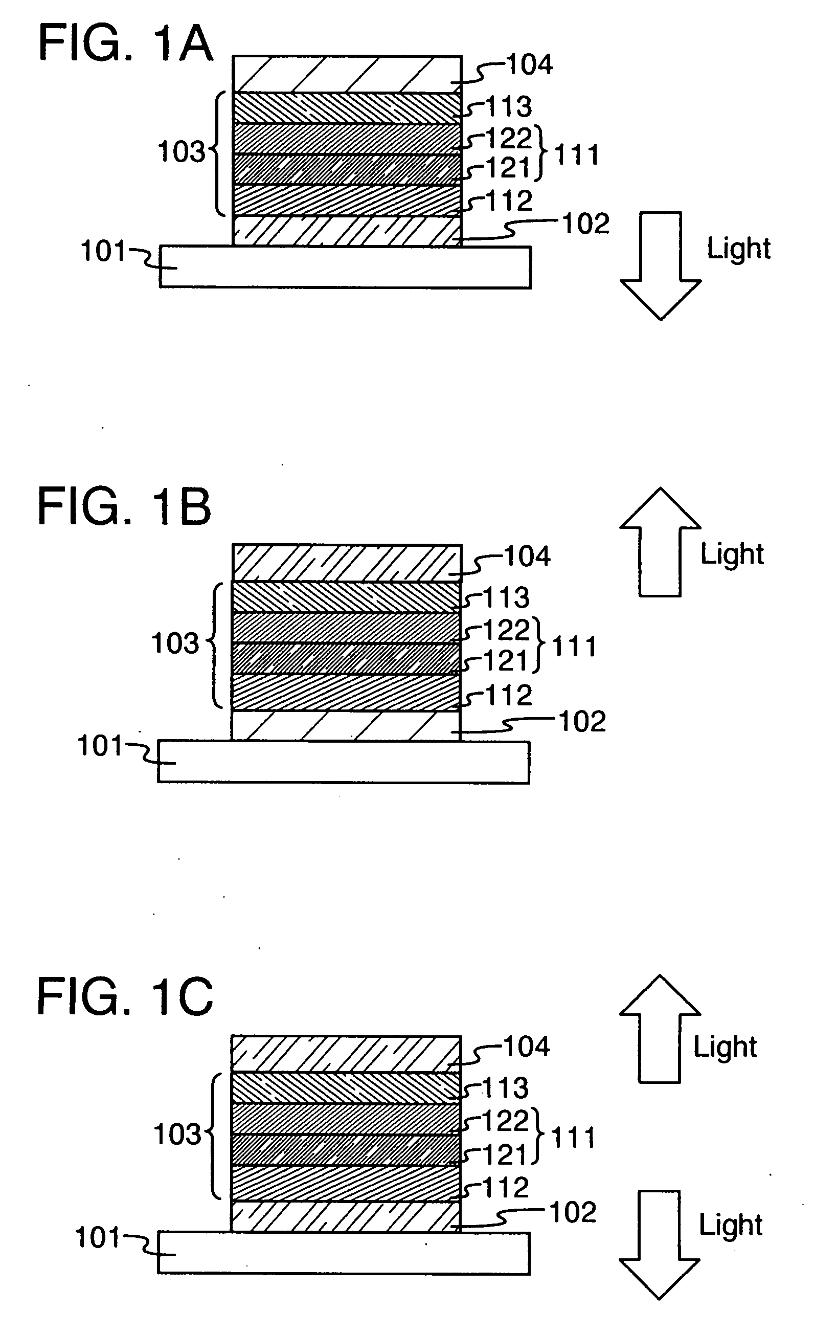
[0051]One mode of a light-emitting element of the present invention will be described with reference to FIG. 1A.

[0052]A light-emitting element of the present invention has a plurality of layers between a pair of electrodes. The plurality of layers are a combination of layers formed of a material with a high carrier injecting property and a material with a high carrier transporting property which are stacked so that a light-emitting region is formed in a region away from the electrodes, that is, recombination of carriers is performed in an area away from the electrodes.

[0053]In this embodiment mode, a light-emitting element includes a first electrode 102, a second electrode 104, and an EL layer 103 provided between the first electrode 102 and the second electrode 104. It is to be noted that the description will be made below regarding the first electrode 102 as an anode and the second electrode 104 as a cathode. In other words, the description will be made below regarding light emiss...

embodiment mode 2

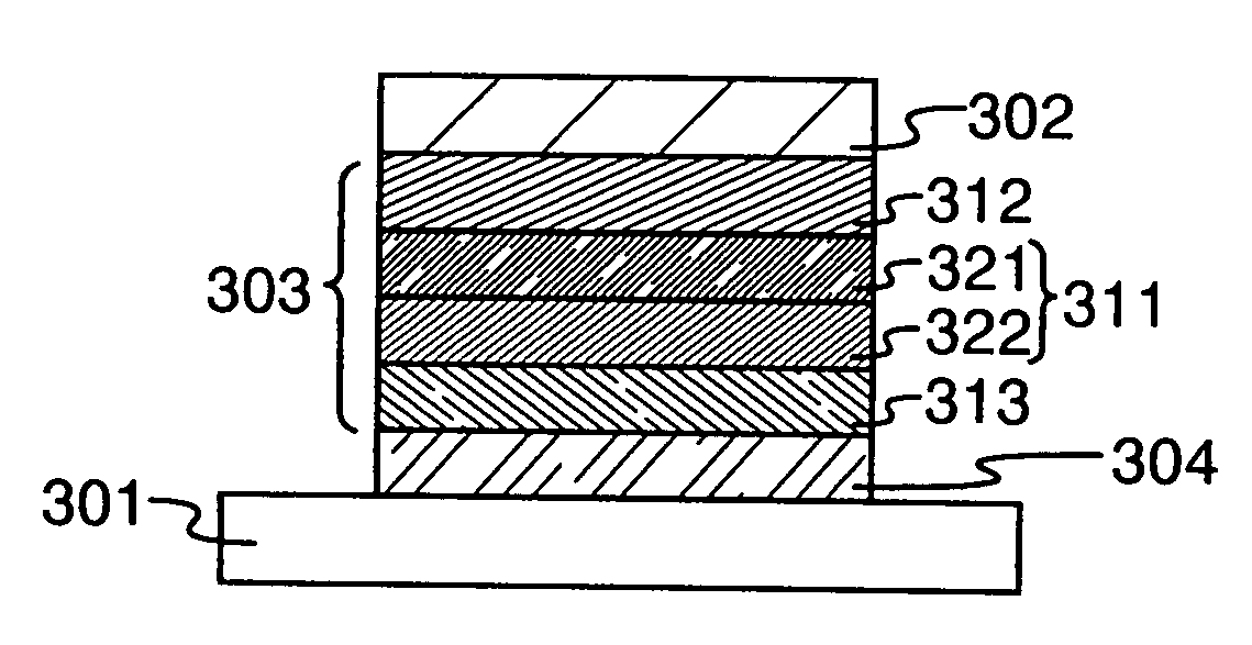
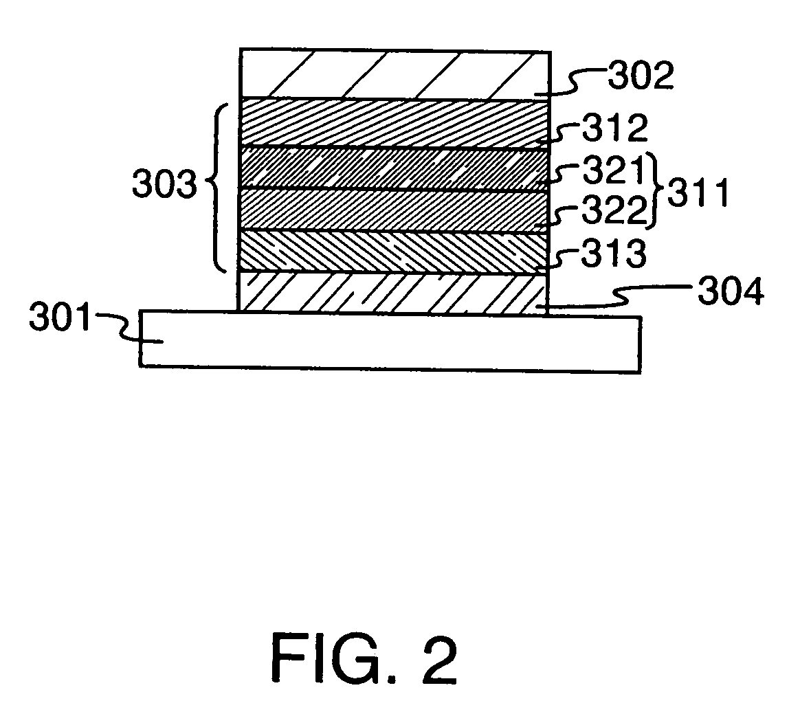
[0091]In this embodiment mode, a mode of a light-emitting element in which a plurality of light-emitting units of the present invention are stacked (hereinafter this light-emitting element is referred to as a stacked-type element) will be described with reference to FIG. 3. The light-emitting element is a stacked-type element including a plurality of light-emitting units between a first electrode and a second electrode. Each of the light-emitting units may have a similar structure to that of the EL layer shown in Embodiment Mode 1. That is, the light-emitting element shown in Embodiment Mode 1 is a light-emitting element having one light-emitting unit, whereas the light-emitting element described in this embodiment mode has a plurality of light-emitting units.

[0092]In FIG. 3, a first light-emitting unit 511 and a second light-emitting unit 512 are stacked between a first electrode 501 and a second electrode 502, and a charge-generating layer 513 is provided between the first light-e...

embodiment mode 3

[0099]In this embodiment mode, a light-emitting device including a light-emitting element of the present invention will be described.

[0100]In this embodiment mode, a light-emitting device including a light-emitting element of the present invention in a pixel portion will be described with reference to FIGS. 4A and 4B. FIG. 4A is a top view showing a light-emitting device, and FIG. 4B is a cross-sectional view taken along a line A-A′ and a line B-B′ in FIG. 4A. Reference numeral 601 denotes a driver circuit portion (source driver circuit), 602 denotes a pixel portion, and 603 denotes a driver circuit portion (gate driver circuit), each of which is shown by a dotted line. Reference numeral 604 denotes a sealing substrate, 605 denotes a sealing member, and 607 denotes a space surrounded by the sealing member 605.

[0101]A lead wiring 608 is a wiring for transmitting signals to be input to the source driver circuit 601 and the gate driver circuit 603, and receives a video signal, a clock ...


PUM


Abstract

A light-emitting element is provided, including a first electrode and a second electrode, a first layer including first and second organic compounds, the first layer being formed between the first electrode and the second electrode wherein the first organic compound is capable of emitting a first light and the second organic compound has an electron transporting property, and a second layer including third and fourth organic compounds, the second layer being formed between the first layer and the second electrode wherein the third organic compound is capable of emitting a second light and has an electron trap property and the fourth organic compound has an electron transporting property.

Description

BACKGROUND OF THE INVENTION[0001]1. Field of the Invention[0002]The present invention relates to a light-emitting element of a current excitation type. Moreover, the present invention relates to a light-emitting device and an electronic device each having the light-emitting element. In more detail, the present invention relates to a long-life light-emitting device which is superior in color purity. Further, the present invention relates to a long-life light-emitting device and electronic device which are superior in color purity.[0003]2. Description of the Related Art[0004]In recent years, research and development have been extensively conducted on light-emitting elements using electroluminescence. As a basic structure of these light-emitting elements, a layer containing a substance with a light-emitting property is interposed between a pair of electrodes. By application of voltage to this element, light emission from a substance with a light-emitting property can be obtained.[0005]...

Claims


Application Information

Patent Timeline
Patent Type & Authority Applications(United States)
IPC IPC(8): H01L29/08H01L35/24H01L51/00
CPCH01L51/0052H01L51/006H01L51/0062H01L51/0067H01L51/5278H01L51/0081H01L51/5012H01L51/5036H01L51/0071H10K85/649H10K85/633H10K85/615H10K85/654H10K85/657H10K85/324H10K50/125H10K50/11H10K50/19Y02B20/30
Inventor SUZUKI, TSUNENORISEO, SATOSHI
Owner SEMICON ENERGY LAB CO LTD
Why Eureka
Try Eureka