Barrier structure and nozzle device for use in tools used to process microelectronic workpieces with one or more treatment fluids
- Summary
- Abstract
- Description
- Claims
- Application Information
AI Technical Summary
Benefits of technology
Problems solved by technology
Method used
Image
Examples
Embodiment Construction
[0070] The embodiments of the present invention described below are not intended to be exhaustive or to limit the invention to the precise forms disclosed in the following detailed description. Rather the embodiments are chosen and described so that others skilled in the art may appreciate and understand the principles and practices of the present invention. While the present invention will be described in the specific context of fluid based microelectronic substrate cleaning systems, the principles of the invention are applicable to other microelectronic processing systems as well.
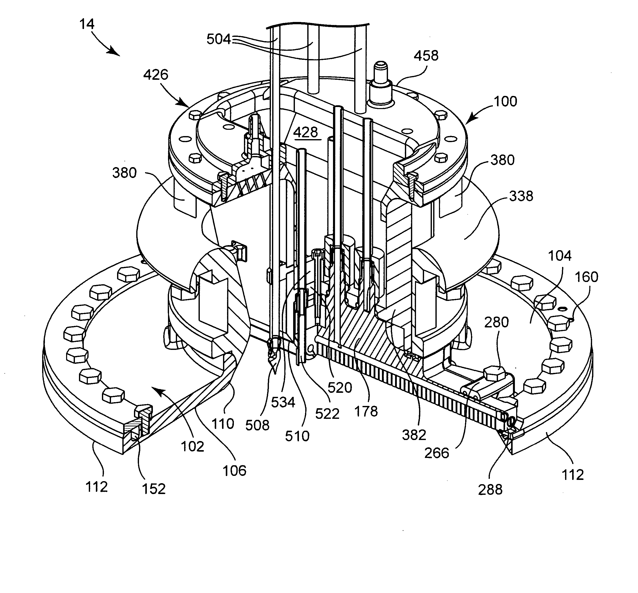
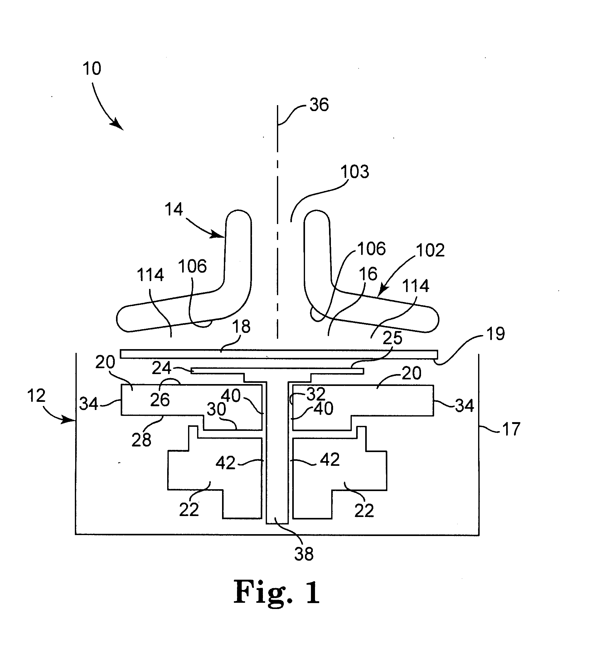
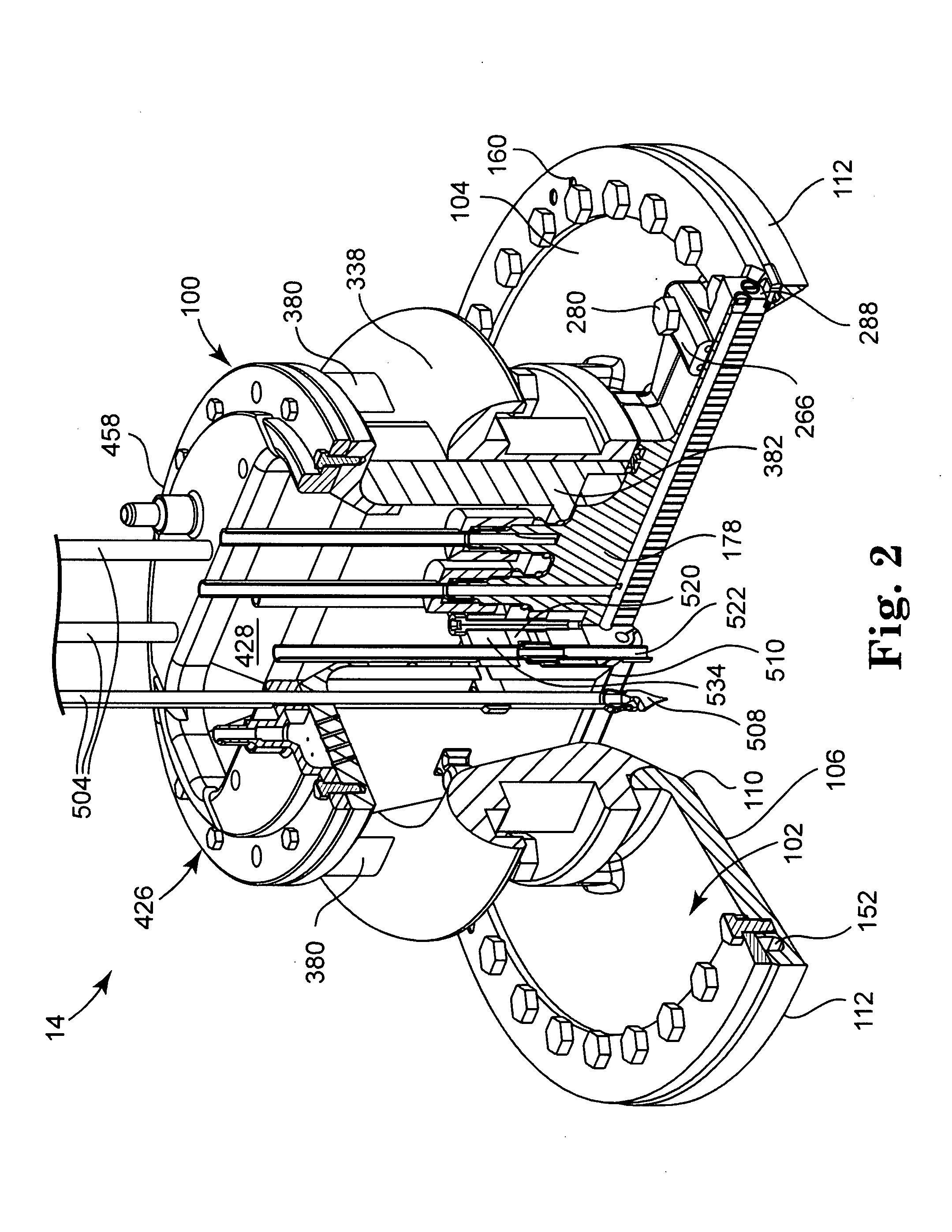
[0071]FIGS. 1 through 37 show an illustrative tool 10 that incorporates principles of the present invention. For purposes of illustration, tool 10 is of the type in which a single workpiece 18 is housed in the tool 10 at any one time and subjected to one or more treatments in which liquid(s), gas(es), and / or other processing media are caused to contact the workpiece 18. In the microelectronics industry, ...
PUM
| Property | Measurement | Unit |
|---|---|---|
| Time | aaaaa | aaaaa |
| Radius | aaaaa | aaaaa |
| Distance | aaaaa | aaaaa |
Abstract
Description
Claims
Application Information


