

Substrate treatment method and film forming method, film forming apparatus, and computer program
a technology of substrate and treatment method, applied in the field of substrate treatment method and film forming method, film forming apparatus, and computer program, can solve problems such as agglutination of cu film, and achieve the effect of increasing the cu film forming ra
- Summary
- Abstract
- Description
- Claims
- Application Information
AI Technical Summary
Benefits of technology
Problems solved by technology
Method used
Image

Examples
Embodiment Construction
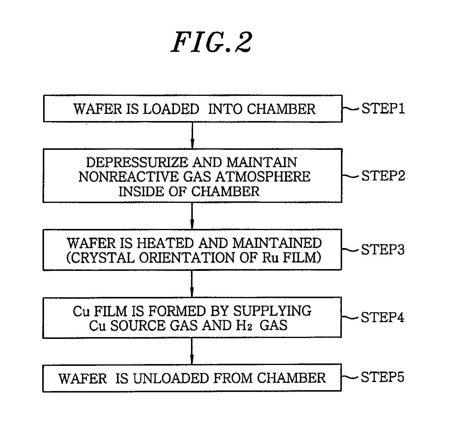
[0024] Hereinafter, embodiments of the present invention will be described with reference to the accompanying drawings.
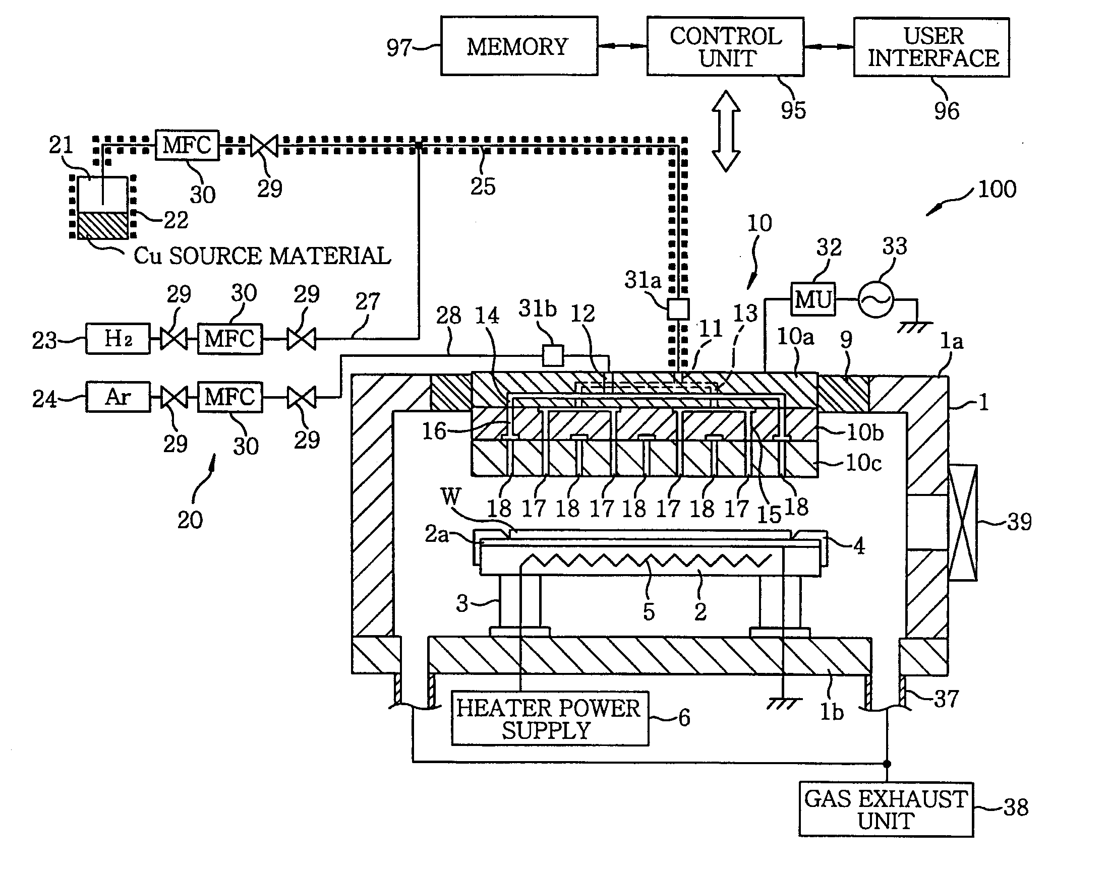
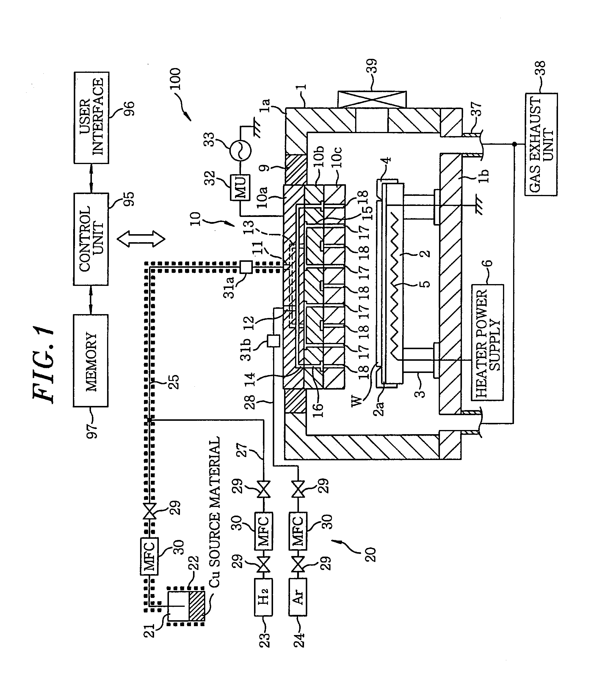
[0025]FIG. 1 is a schematic cross sectional view showing a film forming apparatus 100 for performing a film forming method (including a substrate treatment method) in accordance with an embodiment of the present invention.
[0026] As shown in FIG. 1, the film forming apparatus 100 has a substantially cylindrical chamber 1 which is hermetically sealed. A susceptor 2 for horizontally supporting thereon a wafer W to be processed is disposed in the chamber 1. The susceptor 2 is supported by a cylindrical support member 3. A guide ring 4 for guiding the wafer W is provided at an outer peripheral portion of the susceptor 2. Further, a heater 5 is embedded in the susceptor 2 and connected to a heater power supply 6. By supplying power to the heater 5 from the heater power supply 6, the wafer W is heated up to a specific temperature. Further, the susceptor 2 includes a lowe...
PUM
| Property | Measurement | Unit |
|---|---|---|
| temperature | aaaaa | aaaaa |
| temperature | aaaaa | aaaaa |
| temperature | aaaaa | aaaaa |
Abstract
Description
Claims
Application Information