Vapor deposition mask

A mask and evaporation technology, applied in vacuum evaporation plating, sputtering plating, ion implantation plating and other directions, can solve the problem of inability to reach the substrate, improve service life, avoid board surface deformation, and improve uniformity Effect

Inactive Publication Date: 2013-07-17
KUN SHAN POWER STENCIL
View PDF10 Cites 10 Cited by
  • Summary
  • Abstract
  • Description
  • Claims
  • Application Information

AI Technical Summary

Problems solved by technology

[0014] The technical problem to be solved by the present invention is that in the existing OLED manufacturing technology, the organic particles cannot reach the substrate due to the shielding of the opening wall during evaporation. A new mask for evaporation is provided, which has organic The advantages of high material utilization rate, high film formation rate, long service life of mask plate and cost saving

Method used


Image

  • Vapor deposition mask
  • Vapor deposition mask
  • Vapor deposition mask

Examples


Embodiment 1

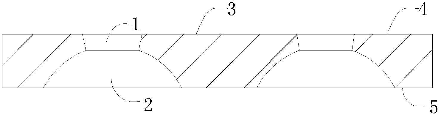
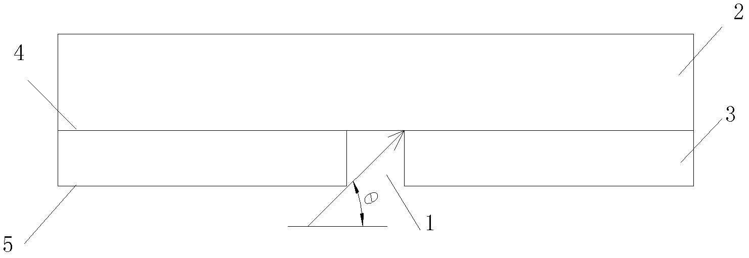
[0030] A mask for evaporation, such as figure 2 As shown, the thickness is 50 μm, and the shape is a quadrilateral Invar alloy plate, including an ITO surface 4 and an evaporation surface 5 that are in contact with an indium tin oxide (ITO) substrate. Through hole, the size of the opening 1 of the through hole on the ITO surface is smaller than the size of the opening 2 on the evaporation surface. Invar alloy is selected as the mask material, and the double-sided etching process is adopted. image 3 It is a schematic diagram of the cooperation between the mask plate and the ITO glass substrate.

[0031] 4 etch from the ITO side of the mask to form as figure 2 Opening 1 on the ITO surface of the middle mask, the depth of opening 1 is 15 μm, and the lateral dimension is 70 μm, etched from the evaporation surface 5 of the mask to form figure 2 Opening 2 on the evaporation surface, and ensure that the center of opening 2 on the evaporation surface coincides with the center o...

Embodiment 2

[0034]A mask for evaporation, with a thickness of 100 μm and a shape of a quadrilateral nickel-cobalt alloy plate, including an ITO surface in contact with an indium tin oxide (ITO) substrate and an evaporation surface, and the mask has a through ITO The size of the opening of the through hole on the ITO surface is smaller than the size of the opening on the evaporation surface.

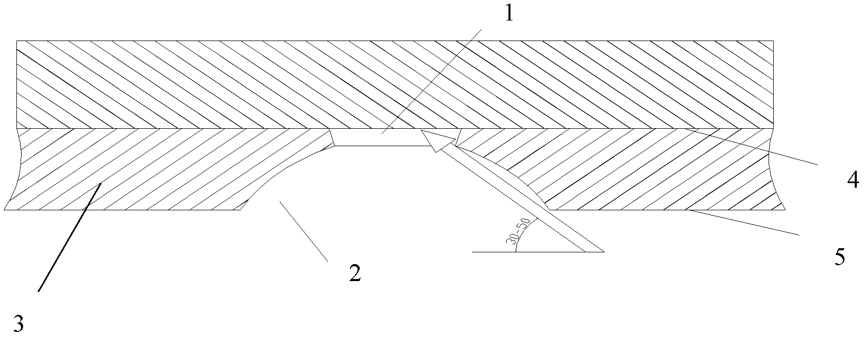
[0035] The mask plate for evaporation is a quadrilateral nickel-cobalt alloy plate, the ITO surface opening depth of the mask plate is 25 μm, and the lateral dimension is 50 μm. The opening on the evaporation surface coincides with the center of the ITO surface opening of the template. The center of the opening is symmetrical, the depth is 75 μm, and the lateral dimension is 100 μm, and the opening wall on the evaporation surface has a certain concave arc, forming an evaporation angle of 30°. By separately controlling the etching time of the ITO surface and the evaporation surface, the required openi...


PUM

PropertyMeasurementUnit
thicknessaaaaaaaaaa
thicknessaaaaaaaaaa

Abstract

The invention relates to a vapor deposition mask, and mainly solves the technical problem that organic particles can not reach a substrate during vapor deposition due to the shielding of a mask opening wall, in a conventional OLED manufacturing technology. The problem is relatively well solved by adopting a technical solution that the vapor deposition mask is a quadrilateral metal plate and comprises an ITO surface contacting with an indium tin oxide (ITO) substrate and a vapor deposition surface; the mask is provided with a through hole penetrating through the ITO surface and the vapor deposition surface; and the opening size of the through hole on the ITO surface is less than the opening size on the vapor deposition surface. The vapor deposition mask can be applied in industrial production of organic light emitting diodes.

Description

[0001] technical field [0002] The invention relates to a mask plate for vapor deposition required in the OLED manufacturing process. [0003] Background technique [0004] Generally, an OLED device is an emissive display device that emits light by electrically exciting a fluorescent organic compound. The OLED device can be regarded as a passive matrix OLED (PMOLED) device or an active matrix OLED (AMOLED) device according to a driving manner of N×M pixels that can be arranged in a matrix. Compared with PMOLED devices, AMOLED devices are suitable for large-sized displays due to their low power consumption and high resolution. [0005] Depending on the direction in which light is emitted from the organic compound, the OLED device can be a top-emitting OLED device, a bottom-emitting OLED device, or a top and bottom-emitting OLED device. Top-emitting OLED devices emit light in the opposite direction to the substrate on which the pixels are disposed and, unlike bottom-emitti...

Claims


Application Information

Patent Timeline
Patent Type & Authority Applications(China)
IPC IPC(8): C23C14/04C23C14/24
Inventor 魏志凌高小平
Owner KUN SHAN POWER STENCIL
Why Eureka
Try Eureka