Universal nucleation layer/diffusion barrier for ion beam assisted deposition

a technology of ion beam and nucleation layer, which is applied in the direction of superconductor devices, instruments, transportation and packaging, etc., can solve the problems of limiting the effective use of this substrate preparation method, affecting the effect of ion beam deposition, etc., to achieve a wide range of thicknesses and vary surface roughness

Inactive Publication Date: 2009-04-30
LOS ALAMOS NATIONAL SECURITY
View PDF9 Cites 7 Cited by
  • Summary
  • Abstract
  • Description
  • Claims
  • Application Information

AI Technical Summary

Benefits of technology

[0018]The invention is a new universal nucleation-layer / diffusion barrier, which is based on amorphous films of Si—O and Si—N for an ion-beam-assisted deposition (IBAD) process. Unlike other nucleation layers that were used in the past, this process works on a variety of substrates (glass, Hastelloy tape, Cu), with varying surface roughness, and with a wide range of thickness. In addition, this new material system of Si—O (and Si—N) is ideally suited for oxide (and nitride) based multilayer stacks. As importantly, the flexibility in nucleation layer thickness allows the nucleation layer to be adjusted to be an effective diffusion barrier, and to be grown at room temperature, while the IBAD layer and subsequent epitaxial layers can be grown much thinner than usual.

Problems solved by technology

Incident ions transfer a significant amount of energy into the substrate resulting in the displacement of target atoms.
The limited depth of the additive with this process, however, can limit the effective use of this substrate preparation method, because substrate surfaces that have a certain roughness may be rendered useless due to the limited depth capability and the inability to smooth over rough surfaces.
However, previous methods have not allowed for a sufficient layer to be applied having a sufficient thickness to correct for any substrates having a rough surface or for substrates that are amorphous such as glass.
Therefore, this limitation has prevented the effective use of the IBAD process on amorphous substrates or substrates that have a rougher surface.
However, when a superconductor crystal is formed on the surface of a metal tape, for example, the deposited crystal layer can hardly be expected to have an oriented structure because such tapes are polycrystalline and also possess a crystal structure different from the deposited oxide superconductor.
Further, thermal processing accompanying the film forming process promotes inter-diffusion of elements between the oxide superconductor and the substrate material, leading to degradation of the oxide material, and the resulting deterioration in the superconducting properties.
Further efforts have resulted in development of a process, coupled with pulsed laser deposition (PLD) YBCO, that has produced meter lengths of superconducting wire with critical current densities over 1 MA / cm2 and critical currents over 100 A. Despite these results, one criticism of the IBAD-YSZ process has been that the time required to deposit the material with sufficient in-plane texture for high quality YBCO is too long.
Thus, the viability of this process has been questionable for cost efficient, industrial fabrication.
However, IBAD MgO still has some drawbacks that detract from its viability as a template layer for long length processing of coated conductors.
The two most detrimental limitations are (1) the degradation of in-plane texture as IBAD MgO film thickness increases beyond a critical thickness of 10 nm; and, (2) the necessity to deposit IBAD MgO films on very smooth (<2 nm rms) substrates.

Method used


Image

  • Universal nucleation layer/diffusion barrier for ion beam assisted deposition
  • Universal nucleation layer/diffusion barrier for ion beam assisted deposition

Examples


Embodiment Construction

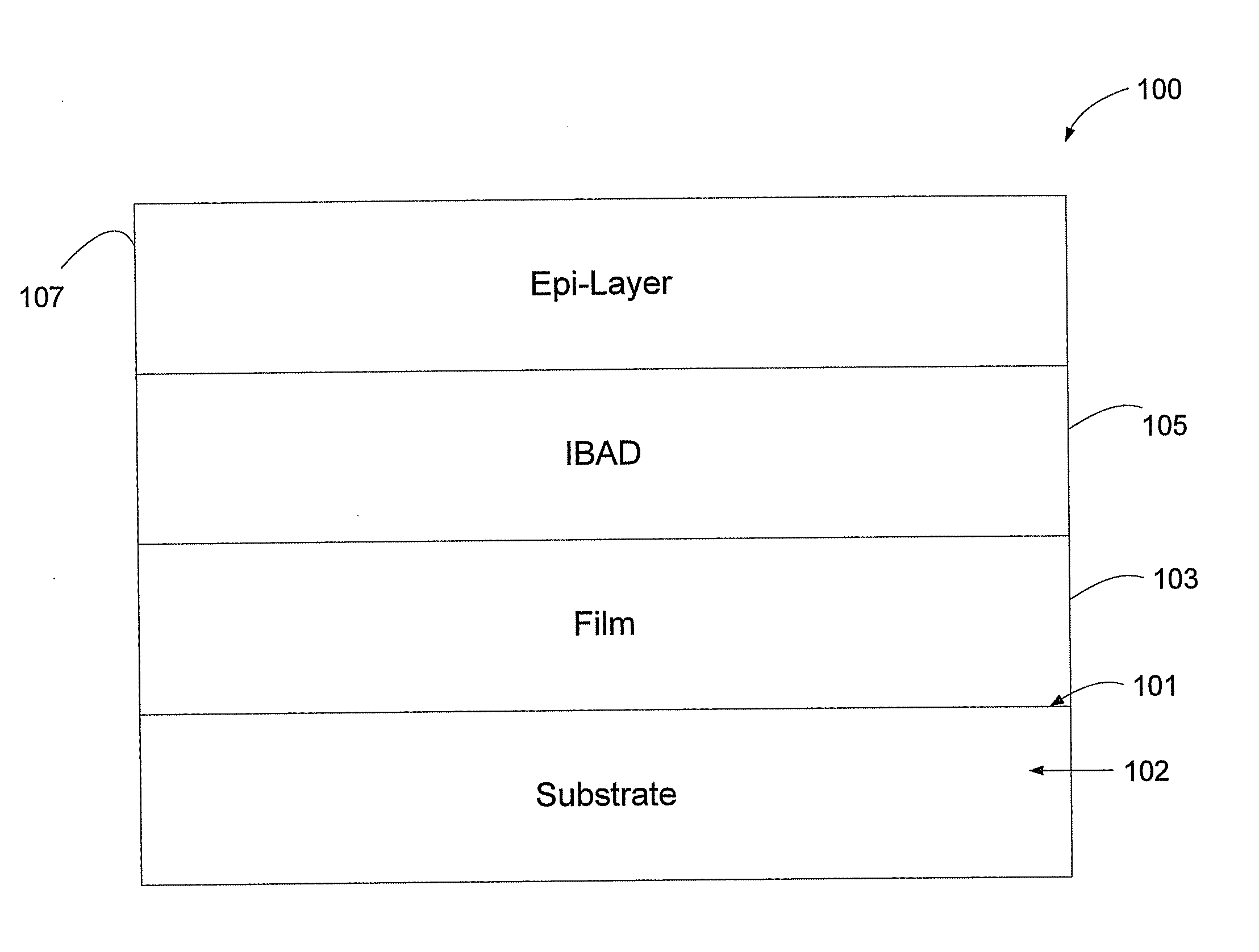
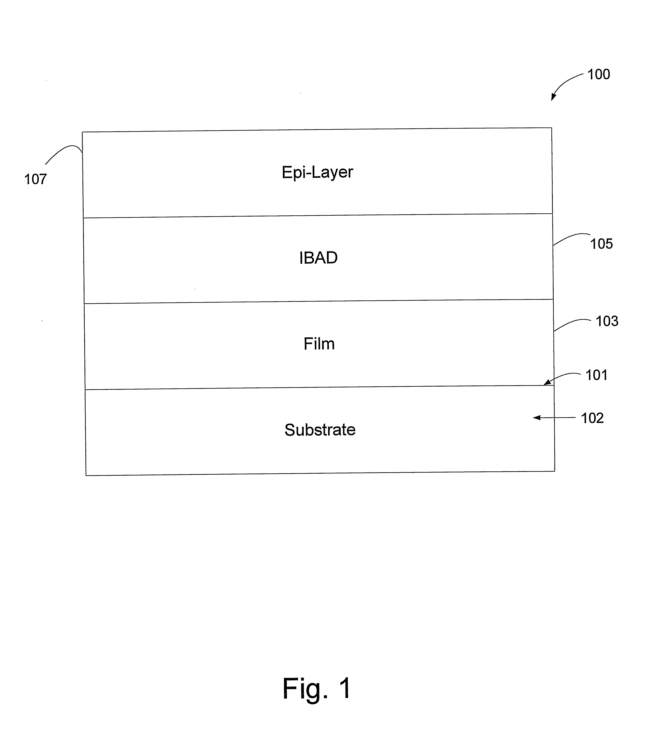
[0033]According to the embodiment(s) of the present invention, various views are illustrated in FIG. 1 and like reference numerals are being used consistently throughout to refer to like and corresponding parts of the invention for all of the various views and figures of the drawing. Also, please note that the first digit(s) of the reference number for a given item or part of the invention should correspond to the Fig. number in which the item or part is first identified.

[0034]One embodiment of the present invention comprising the steps of cleaning a substrate with a 40 mA / 600 eV reactive ion beam with a volumetric flow rate of 5 / 5 / 6 sccm of Ar / Ar / O2 for source / neutralizer / source, respectively for 1 to 5 minutes; depositing 20 to 240 nm of amorphous Si—O at ˜0.2 nm / s with the assistance of the reactive ion beam; and depositing 3 to 6 nm of biaxially-oriented IBAD MgO layer at ˜0.2 nm / s with the assistance of the reactive or inert ion beam using standard conditions and growing homo-e...


PUM

PropertyMeasurementUnit
thicknessaaaaaaaaaa
thicknessaaaaaaaaaa
critical currentsaaaaaaaaaa

Abstract

A method for a new universal nucleation-layer/diffusion barrier, which is based on amorphous films of Si—O and Si—N for ion-beam-assisted deposition (IBAD) process. Unlike other nucleation layers that were used in the past, this process works on a variety of substrates (glass, Hastelloy tape, Cu), with varying surface roughness, and with a wide range of thickness. In addition, this new material system of Si—O (and Si—N) is ideally suited for oxide (and nitride) based multilayer stacks. As importantly, the flexibility in nucleation layer thickness allows the nucleation layer to be an effective diffusion barrier, and to be grown at room temperature, while the IBAD layer and subsequent epitaxial layers can be grown much thinner than usual.

Description

STATEMENT REGARDING FEDERAL RIGHTS [0001]This invention was made with government support under Contract No. DE-AC52-06NA25396 awarded by the U.S. Department of Energy. The government has certain rights in the invention.BACKGROUND OF INVENTION[0002]This invention relates generally to nucleation layers / diffusion barriers and, more particularly, to ion beam assisted deposition.[0003]In many technical thin film deposition processes, ion beam assisted deposition (IBAD) is known to have beneficial effects on the properties of the films. In most of these applications the fast generation of coatings, optical layers, etc., with thickness in the range of microns is at the center of interest. By contrast, when growing epitaxial films in the range of atomic mono layers the layer-by-layer growth mode is most often desired in order to produce films of optimum smoothness. Ion beam assisted deposition techniques are used in the field of integrated semiconductor fabrication for substrate preparation...

Claims


Application Information

Patent Timeline
Patent Type & Authority Applications(United States)
IPC IPC(8): C23C14/14B05D1/36B32B9/04
CPCC23C14/024C23C14/0641Y10T428/265C23C14/221C23C14/081Y10T428/31663H10N60/0632
Inventor FINDIKOGLU, ALP T.
Owner LOS ALAMOS NATIONAL SECURITY
Why Eureka
Try Eureka