Error correction circuit and method, and semiconductor memory device including the circuit

Active Publication Date: 2008-02-28
SAMSUNG ELECTRONICS CO LTD
View PDF7 Cites 30 Cited by
  • Summary
  • Abstract
  • Description
  • Claims
  • Application Information

AI Technical Summary

Benefits of technology

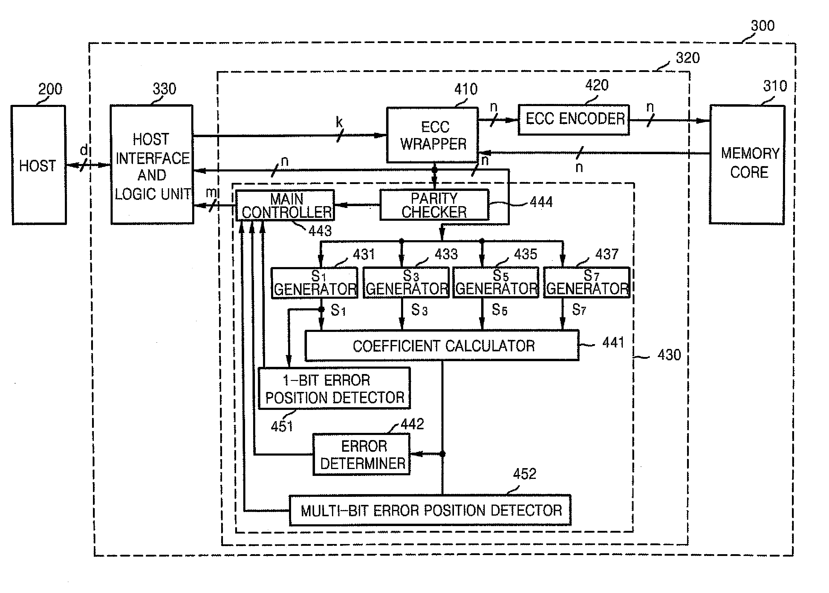
[0015]Embodiments of the present invention decrease data read time and increase read performance by se

Problems solved by technology

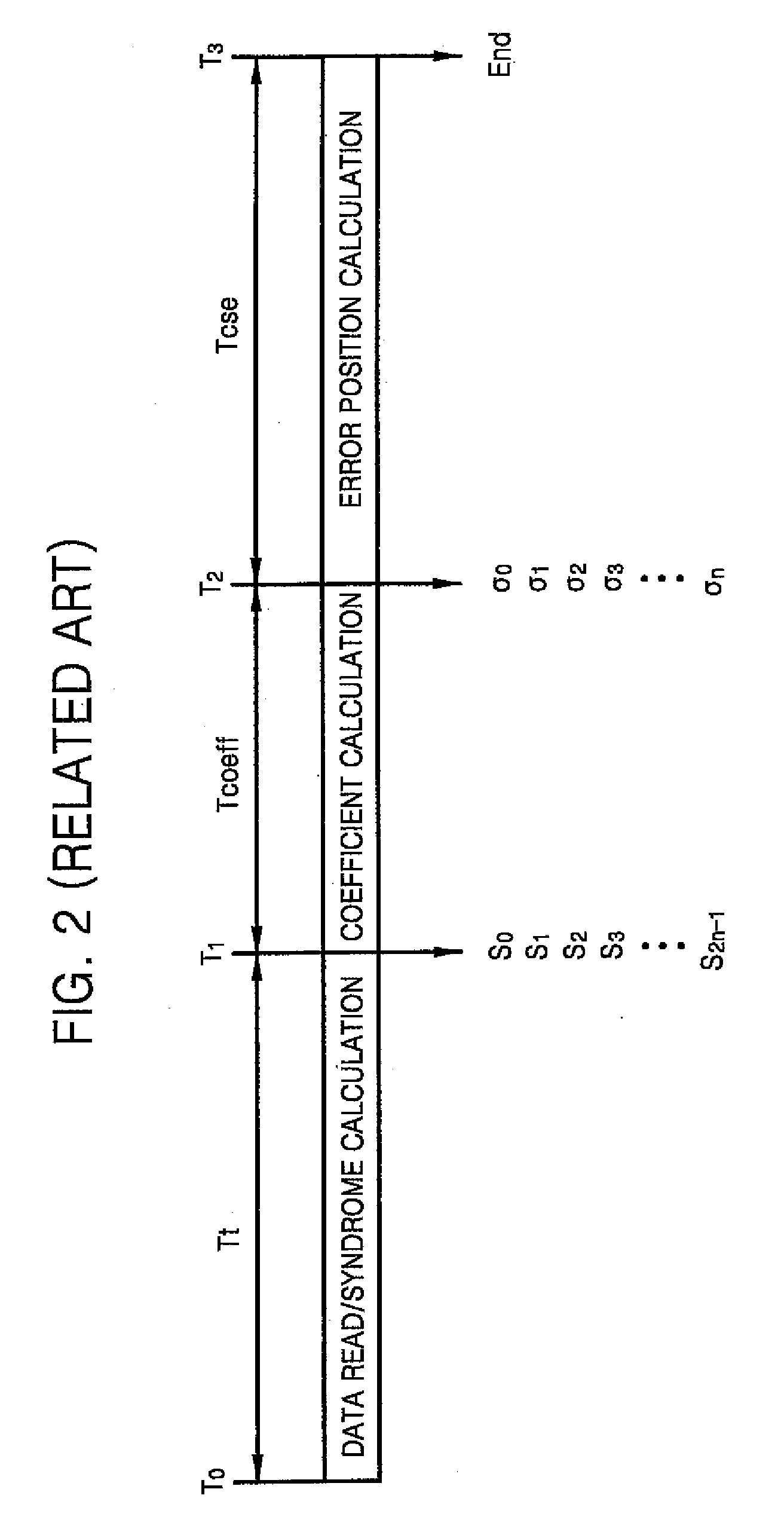
As a consequence, conventional multi-bit ECC circuits and method

Method used


Image

  • Error correction circuit and method, and semiconductor memory device including the circuit
  • Error correction circuit and method, and semiconductor memory device including the circuit
  • Error correction circuit and method, and semiconductor memory device including the circuit

Examples


Example

[0026]The present invention now will be described more fully hereinafter with reference to the accompanying drawings, in which embodiments of the invention are shown. This invention may, however, be embodied in many different forms and should not be construed as limited to the embodiments set forth herein. Rather, these embodiments are provided so that this disclosure will be thorough and complete, and will fully convey the scope of the invention to those skilled in the art. In the drawings, like numbers refer to like elements throughout.

[0027]It will be understood that when an element is referred to as being “connected” or “coupled” to another element, it can be directly connected or coupled to the other element or intervening elements may be present. In contrast, when an element is referred to as being “directly connected” or “directly coupled” to another element, there are no intervening elements present. As used herein, the term “and / or” includes any and all combinations of one ...


PUM


Abstract

An error correction circuit, an error correction method, and a semiconductor memory device including the error correction circuit are provided. The error correction circuit includes a partial syndrome generator, first and second error position detectors, a coefficient calculator, and a determiner. The partial syndrome generator calculates at least two partial syndromes using coded data. The first error position detector calculates a first error position using a part of the partial syndromes. The coefficient calculator calculates coefficients of an error position equation using the at least two partial syndromes. The determiner determines an error type based on the coefficients. The second error position detector optionally calculates a second error position based on the error type. The semiconductor memory device includes the error correction circuit, an error checking and correcting (ECC) encoder generating syndrome data based on information data and generating the coded data by combining the syndrome data with information data, and a memory core storing the coded data. Multi-bit ECC performance is maintained and ECC for a predetermined (1 or 2) or less number of error bits is quickly performed.

Description

BACKGROUND OF THE INVENTION[0001]1. Field of the Invention[0002]The present invention relates to error correction, and more particularly, to an error correction circuit, an error correction method, and a semiconductor memory device including the error correction circuit.[0003]This application claims the benefit of Korean Patent Application No. 10-2006-0080854, filed on Aug. 25, 2006 in the Korean Intellectual Property Office, the disclosure of which is incorporated herein in its entirety by reference.[0004]2. Description of the Related Art[0005]With the increase in memory capacity of a semiconductor memory device, an error correction circuit which can recover an error in a memory cell is required. Conventional error correction circuits may be divided into circuits using a redundant memory cell and circuit using error checking and correction (ECC).[0006]A semiconductor memory device including an error correction circuit using a redundant memory cell includes normal memory cells and r...

Claims


Application Information

Patent Timeline
IPC IPC(8): G06K5/04
CPCG06F11/1008G11C2207/104G11C2029/0411G11C7/1006G11C29/42
Inventor YIM, YONG-TAECHOI, YUN-HO
Owner SAMSUNG ELECTRONICS CO LTD
Why Eureka
Try Eureka