Low voltage column decoder sharing a memory array p-well

Active Publication Date: 2008-05-29
ATMEL CORP
View PDF10 Cites 4 Cited by
  • Summary
  • Abstract
  • Description
  • Claims
  • Application Information

AI Technical Summary

Benefits of technology

[0013]The present invention describes an architecture to minimize the footprint of the column decoder of a memory device and to increase the speed performance of the access path.
[0020]An advantage of an architecture according to the present invention are that the first levels of the column decoder, which have the highest number of selectors in the hierarchical decoding, are realized by means of low-voltage MOS (LVMOS) devices. Low-voltage MOS devices minimize the overall footprint of a column decoder and increasing the performance of the read access path. High-voltage (HVMOS) devices are only needed in the last hierarchical decoder level, which has the lower number of selector transistors. As a consequence, the lower number of threes last HVMOS devices can have their dimensions increased, if desired, to improve their speed performance with a minimum impact on the overall footprint of the column decoder circuitry.

Problems solved by technology

This type of high-voltage MOS (HVMOS) transistor has a huge area footprint and poor performance compared with the low-voltage MOS (LVMOS) type of transistors needed for just reading the memory cells.

Method used


Image

  • Low voltage column decoder sharing a memory array p-well
  • Low voltage column decoder sharing a memory array p-well
  • Low voltage column decoder sharing a memory array p-well

Examples


Embodiment Construction

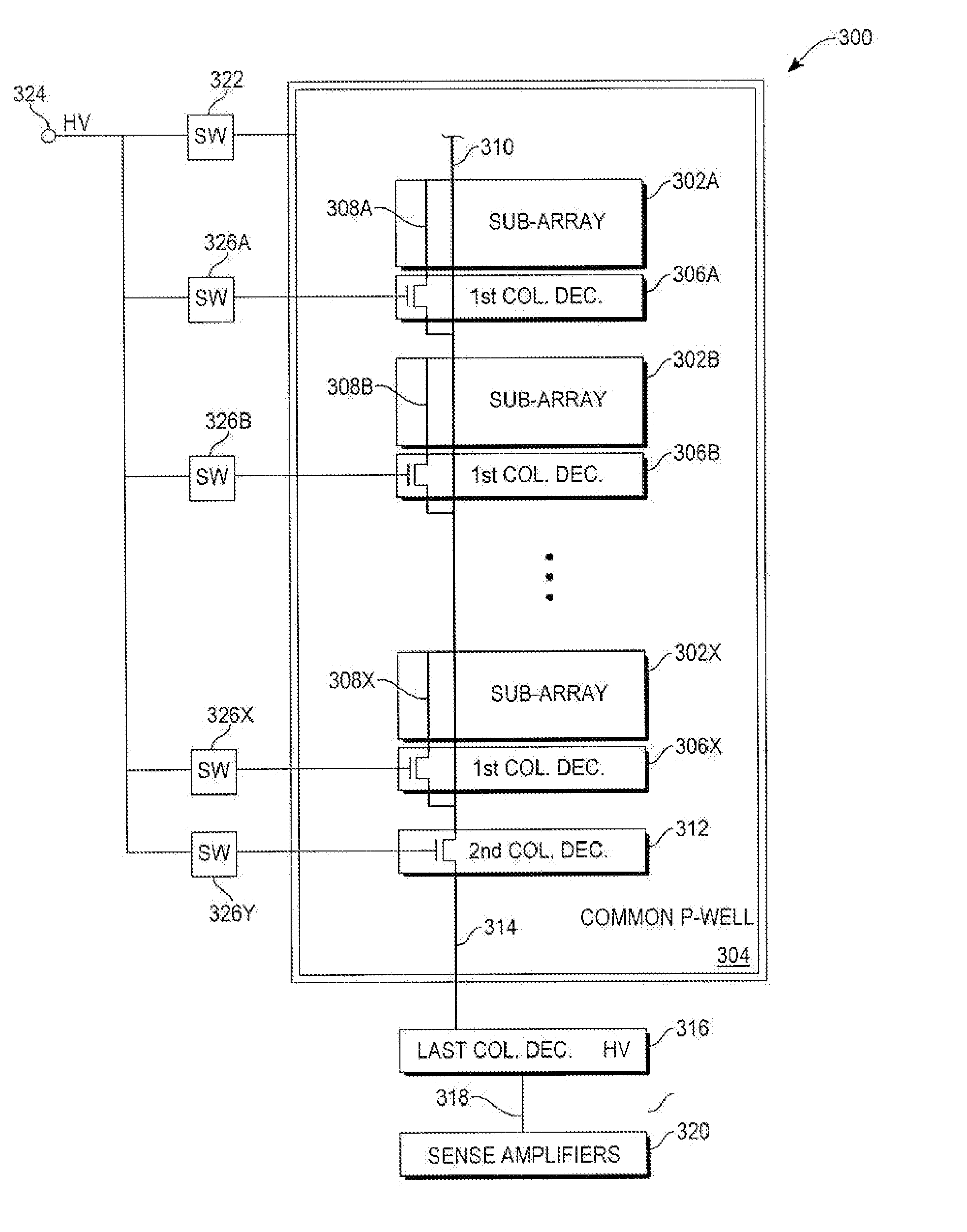
[0030]The present invention provides a memory configuration that reduces the footprint of a column decoder for a memory device, while increasing the speed of the access path to the memory.

[0031]FIG. 6 illustrates one embodiment of the present invention. A memory device 300 is provided with a plurality of sub-arrays 302A, 302B, . . . , 302x that share a common p-well region 304. A first level of column decoders 306A, 306B, . . . , 306x within the common p-well region 304 provide selected connections from local column lines 308A, 308B, . . . , 308x in the memory sub-arrays to a global column line 310.

[0032]To illustrate additional hierarchical levels of decoding, a second-level column decoder 312 shown inside the same common p-well region 304. Note that other levels of column decoders inside the same memory p-well region 304 may be added according to the number n of columns and m of sense amplifiers required. The second-level column decoder 312 has a global column line 314.

[0033]The l...


PUM


Abstract

A plurality of memory sub-arrays are formed in a p-well region. Each of the memory sub-arrays has at least one first-level column decoder that includes a plurality of low-voltage MOS selector transistors that are also formed within the p-well. A last-level decoder is formed outside of the p-well region and includes high-voltage MOS transistors to provide an output signal to one of an array of sense amplifiers. During a memory erase mode of operation, a high voltage is provided to bias the p-well region and a plurality of high-voltage switches are activated to provide a high voltage to gate terminals of the selector transistor in the first-level column decoders. One or more intermediate-level column decoders are formed as low-voltage selector transistors in the p-well between the first-level column decoder and the last-level column decoder. Each of the intermediate-level column decoders also has a high-voltage switch that is activated during a memory erase mode of operation to provide a high voltage to gate terminals of the intermediate-level column decoders.

Description

TECHNICAL FIELD[0001]The present invention relates to non-volatile memories having a hierarchical address decoding organization.BACKGROUND ART[0002]Non-volatile memory devices are widely used in portable systems, such as, for example, laptop computers, personal digital assistants (PDAs), mobile telephones, and various other portable devices and systems. Most of these non-volatile memory devices require a high voltage supply that is internally generated to optimize power consumption of a portable device and that provides a system designer with more. Non-volatile memories store binary information whether or not power is supplied to the memory, which is very useful in portable systems.[0003]Non-volatile memories are realized using floating gate devices, which store information by changing their physical state to two or more physical states. Different physical states are obtained by changing the threshold voltage of the floating gate device by means of injection and extraction of electr...

Claims


Application Information

Patent Timeline
IPC IPC(8): G11C16/14G11C16/04
CPCG11C16/08
Inventor FRULIO, MASSIMILIANOSURICO, STEFANOSACCO, ANDREAMANFRE, DAVIDE
Owner ATMEL CORP
Why Eureka
Try Eureka