Chip package and digital camera module using same

Inactive Publication Date: 2008-03-06
ALTUS TECH INC
View PDF5 Cites 5 Cited by
  • Summary
  • Abstract
  • Description
  • Claims
  • Application Information

AI Technical Summary

Problems solved by technology

The dust-particles may obscure the optical path and produce errors in the image sensing process.
Accordingly, the quality and/or reliability of the chip package 10 may be adversely affected.
Furthermore, it is difficult to ensure that an optical axis of the lens module 14 is precisely aligned with a center of the active area 1051 of th

Method used


Image

  • Chip package and digital camera module using same
  • Chip package and digital camera module using same
  • Chip package and digital camera module using same

Examples


Embodiment Construction

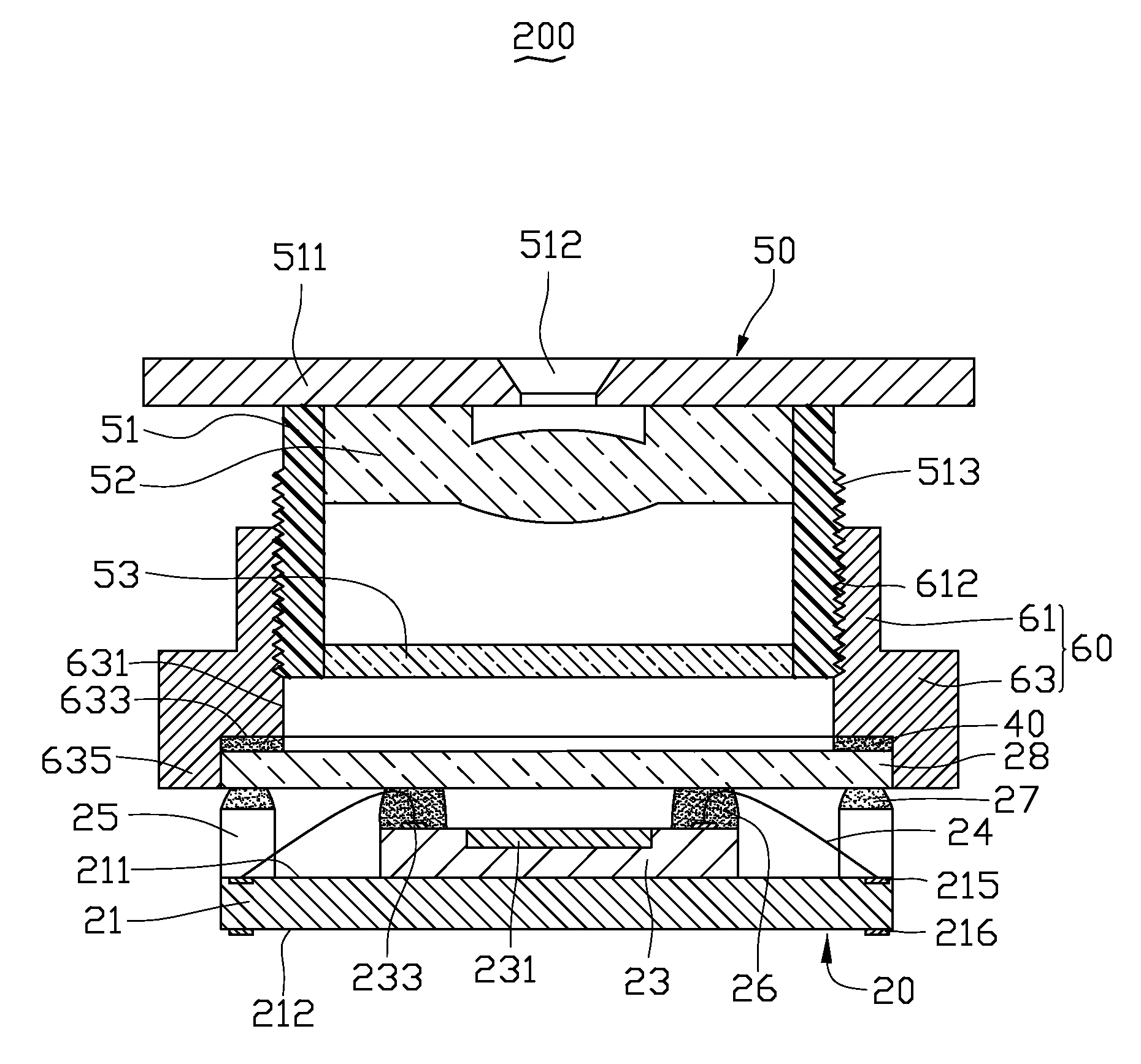
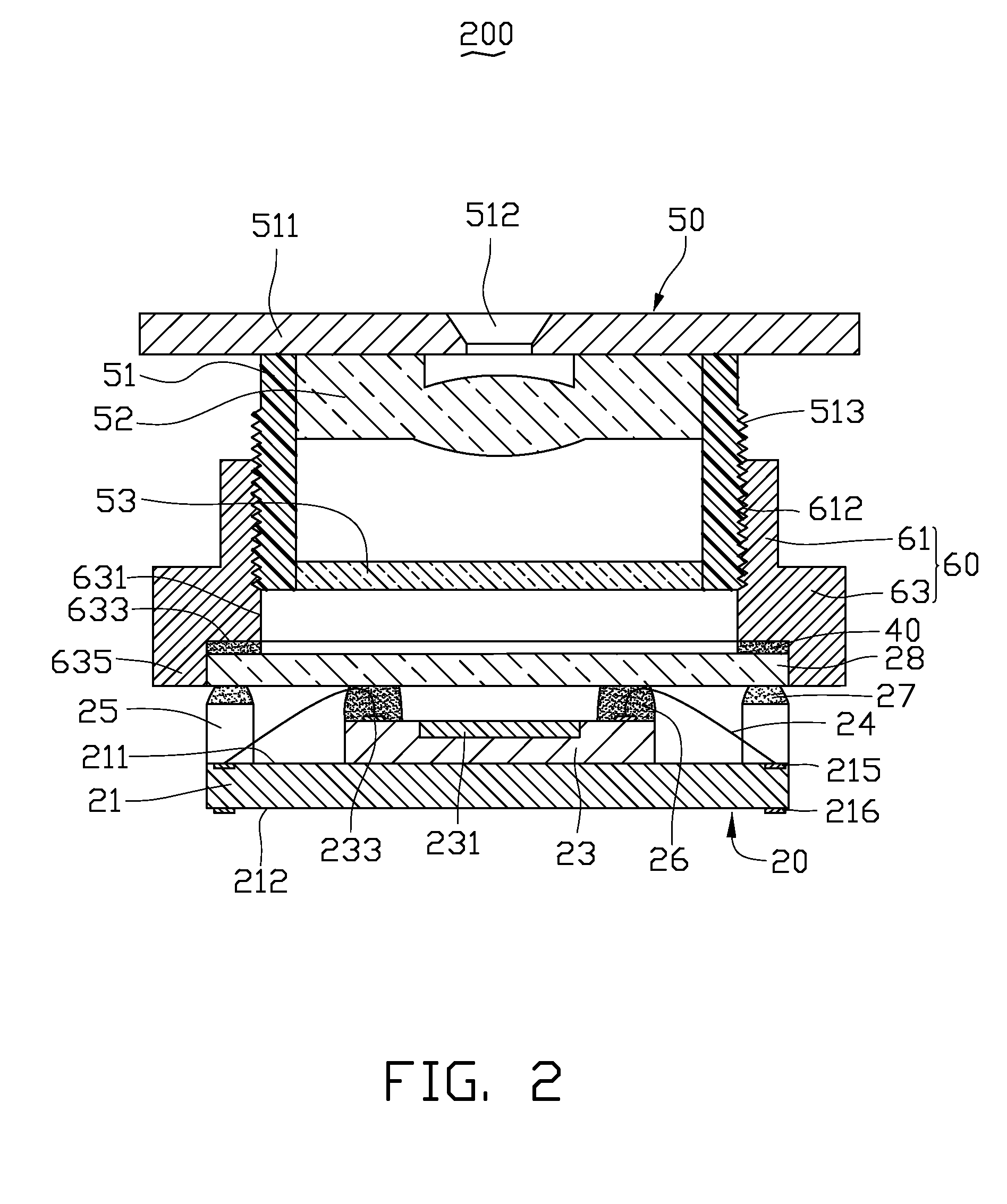
[0018]Referring to FIG. 2, a digital camera module 200 having a chip package 20 according to a preferred embodiment of the present invention is shown. The digital camera module 20 includes the chip package 20, a third adhesive 40, a lens module 50, and a holder 60.

[0019]The chip package 20 includes a carrier 21, a chip 23, a plurality of wires 24, a supporting member 25, a first adhesive 26, a second adhesive 27, and a cover 28.

[0020]Referring to FIGS. 2 and 3, the carrier 21 has an approximately planar top surface 211, a bottom surface 212 positioned opposite to the top surface 212, a plurality of top contacts 215 arranged on the top surface 211, and a plurality of bottom contacts 216 disposed on the bottom surface 212. Each top contact 215 electrically connects with a corresponding bottom contact 216 via a respective interconnecting device (not shown). The top and bottom contacts 215, 216 are both configured for electrically connecting with other electronic components, for example...


PUM


Abstract

A digital camera module (200) includes a chip package (20) and a lens module (50) mounted to the chip package. The package includes a carrier (21), a chip (23), a plurality of wires (24), a supporting member (25), an adhesive (26), and a cover (28). The carrier has a top surface (211), and a plurality of top contacts (215) arranged on the top surface. The chip is mounted to the top surface of the carrier, and includes an active area (231) and a plurality of pads (233). The wires electrically respectively connect one of the pads to a corresponding top contact. The adhesive is applied to a peripheral circumference of the top surface of the chip. The cover is adhered to the adhesive, and closes the active area of the chip. The supporting member is disposed between the carrier and the cover to support the cover.

Description


Claims


Application Information

Patent Timeline
Owner ALTUS TECH INC
Why Eureka
Try Eureka