Electrostatic discharge protection circuit for compound semiconductor devices and circuits

a protection circuit and semiconductor technology, applied in the field of semiconductor devices, can solve the problems of destroying devices and circuits that are not protected from esd events, and affecting the performance of semiconductor devices and other integrated circuits

Active Publication Date: 2008-03-13
QORVO US INC
View PDF16 Cites 71 Cited by
  • Summary
  • Abstract
  • Description
  • Claims
  • Application Information

AI Technical Summary

Problems solved by technology

Semiconductor devices and other integrated circuits are susceptible to damage from an electrostatic discharge (ESD) event.
An ESD event occurs when a high potential voltage and current are rapidly discharged into the device or circuit, which typically results in the destruction of devices and circuits that are not protected from ESD events.
The use of diodes in the discharge path to dissipate an ESD event is disadvantageous due to the series resistance of each diode.
This affects the ability of the ESD protection device to dissipate an ESD event as rapidly as possible.
Another disadvantage of ESD protection circuit 100 is that it uses large diodes (i.e., diodes that have large widths) in order to effectively dissipate an ESD event.
Among other things, large diodes consume a relatively large amount of area in the component that contains the ESD protection circuit.
Consequently, the component must be larger, which, among other things, increases the cost of the component.
Consequently, the use of the transistor and resistor, rather than a multiplicity of diodes, is still disadvantageous for the reasons described above.
Among other things, the need for power supplies increases the complexity, and therefore the cost, of the ESD protection circuit, because additional terminals are needed to connect the power supplies to the ESD protection circuit.
One disadvantage of such an ESD protection circuit is that it requires two separate discharge paths, one to dissipate a positive ESD event and another to dissipate a negative ESD event.
Among other things, the presence of two discharge paths adds complexity to the ESD protection circuit, consumes space, and increases the cost of the ESD protection circuit.
This increases the series resistance in the discharge path, which, as described above, is a disadvantage for ESD protection circuits.

Method used


Image

  • Electrostatic discharge protection circuit for compound semiconductor devices and circuits
  • Electrostatic discharge protection circuit for compound semiconductor devices and circuits
  • Electrostatic discharge protection circuit for compound semiconductor devices and circuits

Examples


Embodiment Construction

[0017]Reference will now be made to the following detailed description of embodiments of the present invention. Those skilled in the art will recognize that embodiments of the present invention provide many inventive concepts and novel features that are merely illustrative, and are not to be construed as restrictive. Accordingly, the specific embodiments described herein are given by way of example and do not limit the scope of the embodiments of the present invention. In addition, those skilled in the art will understand that for purposes of explanation, numerous specific details are set forth, though embodiments of the invention can be practiced without these specific details, and that certain features have been omitted so as to more clearly illustrate embodiments of the present invention.

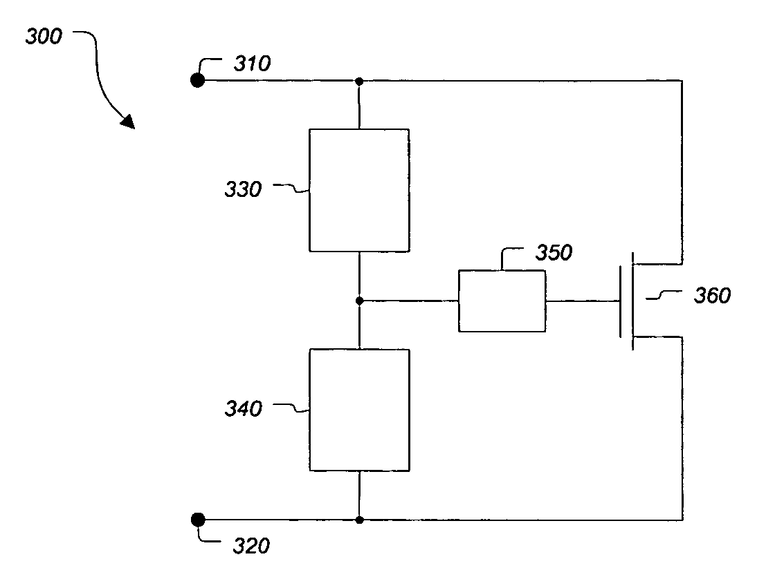
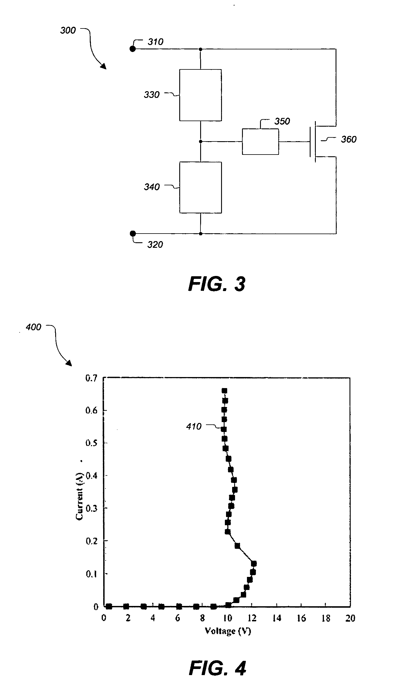
[0018]FIG. 3 illustrates a block diagram of an electrostatic discharge (ESD) protection circuit 300 according to an embodiment of the present invention. ESD protection circuit 300 comprises termi...


PUM


Abstract

An apparatus and method is disclosed for providing an electrostatic discharge protection circuit for compound semiconductor devices and circuits. The electrostatic discharge protection circuit comprises a first terminal and a second terminal. The electrostatic discharge protection circuit further comprises a transistor shunt element that is operably coupled between the first terminal and the second terminal; the transistor shunt element is capable of providing a bi-directional discharge path between the first terminal and the second terminal. The electrostatic discharge protection circuit further comprises a shut-off element that is operably coupled with the second terminal; the shut-off element is capable of keeping the transistor shunt element turned-off.

Description

TECHNICAL FIELD OF THE INVENTION[0001]Embodiments of the present invention relate generally to semiconductor devices and more specifically, to an electrostatic discharge protection circuit for compound semiconductor devices and circuits.BACKGROUND OF THE INVENTION[0002]Semiconductor devices and other integrated circuits are susceptible to damage from an electrostatic discharge (ESD) event. For example, an ESD event may occur either during the assembly and packaging of these devices and circuits, or during normal operation of these devices and circuits in an end product. An ESD event occurs when a high potential voltage and current are rapidly discharged into the device or circuit, which typically results in the destruction of devices and circuits that are not protected from ESD events.[0003]FIG. 1 shows a schematic diagram of an ESD protection circuit according to the prior art. ESD protection circuit 100 includes an input / output pad 110, an internal circuit 120, and a multiplicity ...

Claims


Application Information

Patent Timeline
Patent Type & Authority Applications(United States)
IPC IPC(8): H02H9/00
CPCH02H9/046H01L27/0266
Inventor PING, ANDREW T.OGBONNAH, DOMINIC J.
Owner QORVO US INC
Why Eureka
Try Eureka