Image processing device, image processing method, recording medium, and program

a technology of image processing and image processing method, which is applied in the field of image processing device, image processing method, recording medium, and program, can solve the problems of increasing power consumption and noise, reducing the speed of high-speed readout operations, and reducing the deformation and distortion of subject images

Inactive Publication Date: 2008-04-24
SONY CORP
View PDF4 Cites 27 Cited by
  • Summary
  • Abstract
  • Description
  • Claims
  • Application Information

AI Technical Summary

Problems solved by technology

However, with the technique described in Japanese Unexamined Patent Application Publication No. 2004-140479, high-speed readout operations so fast that deformation and distortion of subject images become negligible become extremely difficult as the number of pixels increases, and further, power consumption and noise increase.
In other words, high-speed readout within a range wherein increased power consumption and noise can be suppressed does not exhibit sufficient alleviation of deformation and distortion of subject images.
Also, the techniques described in Japanese Unexamined Patent Application Publication Nos. 2004-140149, 2004-159555, and 2005-65074 involve increasing the pixel size, so there are restrictions that this cannot be applied to small image sensors with a great number of pixels.
Also, the technique described in Japanese Unexamined Patent Application Publication No. 2006-58945 requires a reference image for correcting taken images, and accordingly cannot be used for general-purpose applications.

Method used


Image

  • Image processing device, image processing method, recording medium, and program
  • Image processing device, image processing method, recording medium, and program
  • Image processing device, image processing method, recording medium, and program

Examples


Embodiment Construction

[0087] Before describing an embodiment of the present invention, the correspondence between the features of the claims and the specific elements disclosed in an embodiment of the present invention is discussed below. This description is intended to assure that an embodiment supporting the claimed invention is described in this specification. Thus, even if an element in the following embodiment is not described as relating to a certain feature of the present invention, that does not necessarily mean that the element does not relate to that feature of the claims. Conversely, even if an element is described herein as relating to a certain feature of the claims, that does not necessarily mean that the element does not relate to the other features of the claims.

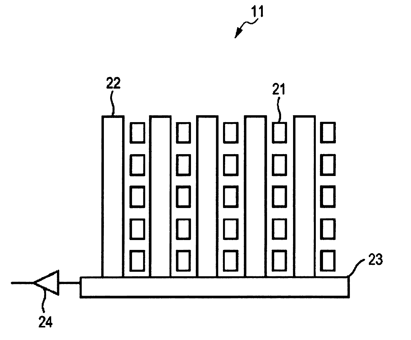
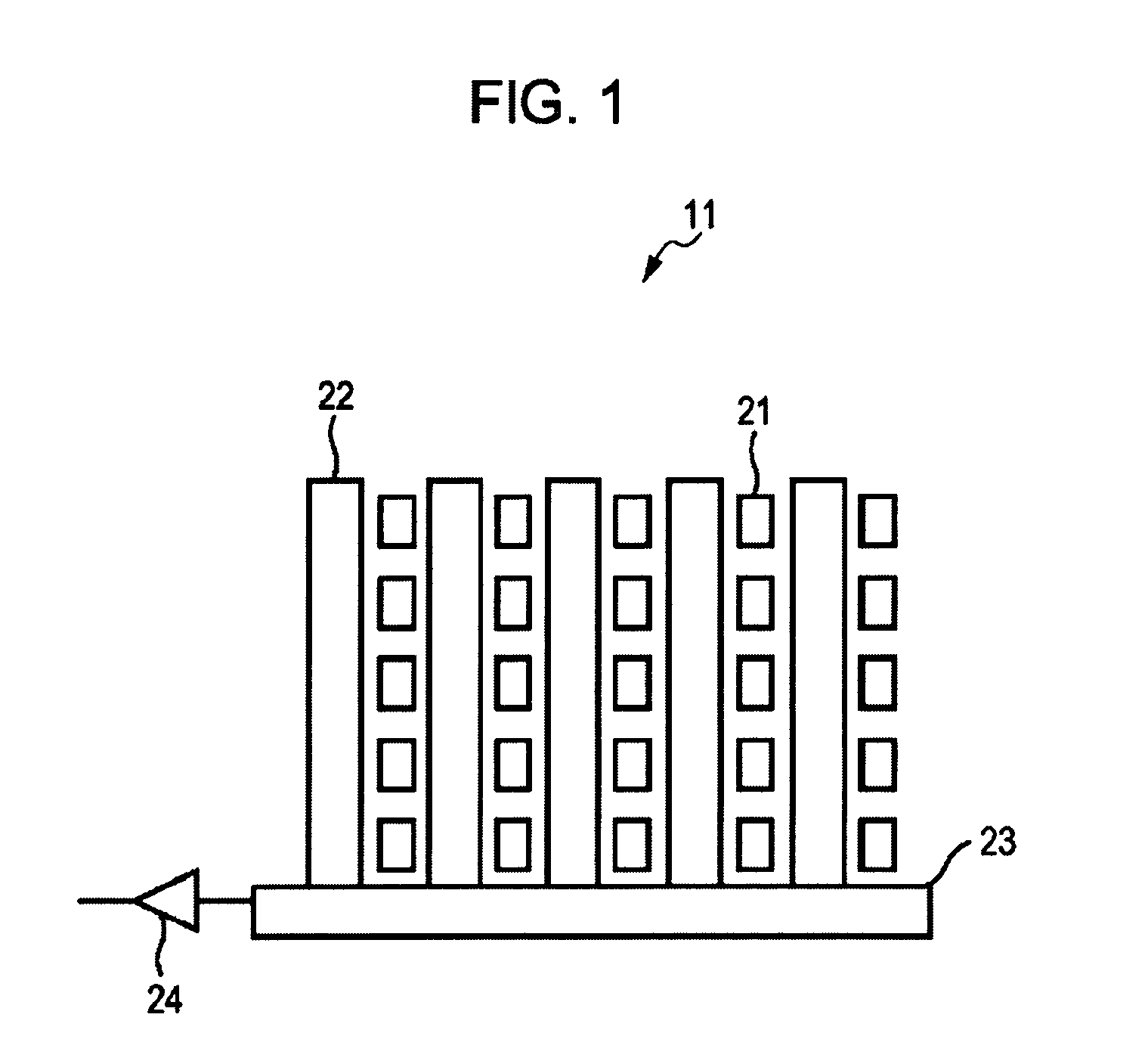
[0088] An image processing device according to an embodiment of the present invention includes: an image acquisition unit (e.g., a pre-processing unit 101 in FIG. 9 or FIG. 23), for acquiring a plurality of image data sets config...


PUM


Abstract

An image acquisition unit acquires multiple image data sets of pixels in array, having subject distortion due to focal plane shutter effects, corresponding to images taken at continuous exposure timings; a coefficient storage unit stores coefficients, determined by which number-in-order of multiple images that the image data set corresponds to, and by each pixel position in the image; a multiplying unit multiplies a pixel value of a predetermined pixel in the image data sets, by the coefficient stored in the coefficient storage means; and an adding unit adds each pixel value of a predetermined number of the image data sets. The coefficients include a coefficient wherein, at the earliest image data set, pixels exposed earlier are weighted less and pixels exposed later are weighted more, and a coefficient wherein, at the latest image data set, pixels exposed earlier are weighted more and pixels exposed later are weighted less.

Description

CROSS REFERENCES TO RELATED APPLICATIONS [0001] The present invention contains subject matter related to Japanese Patent Application JP 2006-066929 filed in the Japanese Patent Office on Jun. 16, 2006, the entire contents of which are incorporated herein by reference. BACKGROUND OF THE INVENTION [0002] 1. Field of the Invention [0003] The present invention relates to an image processing device, an image processing method, a recording medium, and a program, and more particularly relates to an image processing device, an image processing method, a recording medium, and a program, capable of correcting distortion due to focal plane shutter effects in a taken image. [0004] 2. Description of the Related Art [0005] The principle of readout from a CCD image sensor 11 will be described with reference to FIGS. 1 through 2C. [0006] The CCD image sensor 11 includes photodiodes 21, vertical CCDs 22, a horizontal CCD 23, and an output amplifier 24. [0007] As shown in FIG. 2A, at the CCD image se...

Claims


Application Information

Patent Timeline
Patent Type & Authority Applications(United States)
IPC IPC(8): H04N5/228G06T1/00H04N5/232
CPCH04N5/232H04N5/23248H04N5/23232H04N23/951H04N23/68
Inventor YOSHIMURA, SHINICHI
Owner SONY CORP
Why Eureka
Try Eureka