Method for producing a layer arrangement

a layer arrangement and manufacturing method technology, applied in the direction of semiconductor/solid-state device manufacturing, basic electric elements, electric apparatus, etc., can solve the problems of high chip area cost, inability to optimally patterned, and interrupt the routing in the design, so as to improve contact

Active Publication Date: 2008-05-01
INFINEON TECH AG
View PDF13 Cites 2 Cited by
  • Summary
  • Abstract
  • Description
  • Claims
  • Application Information

AI Technical Summary

Benefits of technology

[0027]The invention is based, in particular, on the object of providing a method for producing a layer arrangement providing for improved contacting between different electrically conductive patterns.

Problems solved by technology

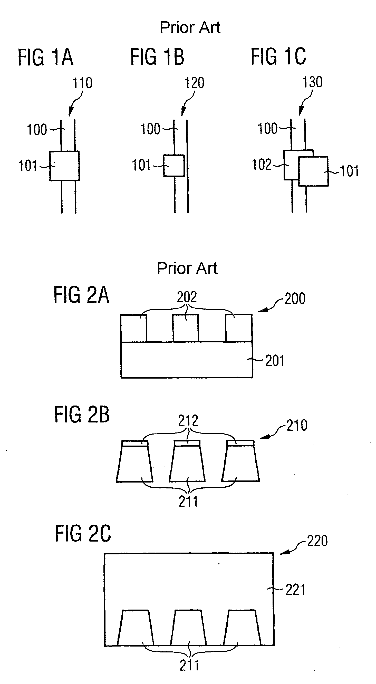
Due to process-related fluctuations in the adjustment of etching masks for vias, however, these cannot be patterned optimally but only with a certain, for example lateral offset.
The larger areas lead to a lateral winding of the metal tracks in the environment of the vias which interrupts the routing in the design.
This is disadvantageous with regard to the high costs of chip area since it increases the space required for an integrated circuit.
This additional expenditure in the layout and the associated loss in chip area is disadvantageous with regard to the requirement for ICs with increasingly greater integration.
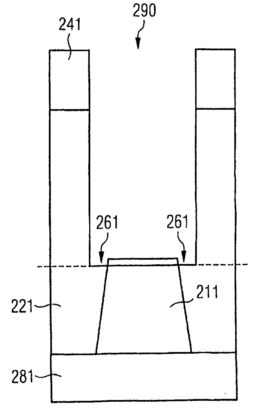
These narrow gaps 261 are the cause of many problems which lead to severe reliability problems.
Thus, polymer material in the gaps 261 can only be cleaned or removed incompletely or not at all.
This leads to problems in a subsequent liner deposition and / or metal filling for forming the vias.
Furthermore, adhesive, seed or barrier layers, called liners, can only be deposited incompletely when narrow gaps 261 occur.
This leads to unreliable contacting between metal tracks 211 and vias.
This leads to problems with regard to the quality of the layer arrangement 270 with regard to its use as integrated circuit.
There is always deep etching-in next to the metal track which then leads to the problems described above.
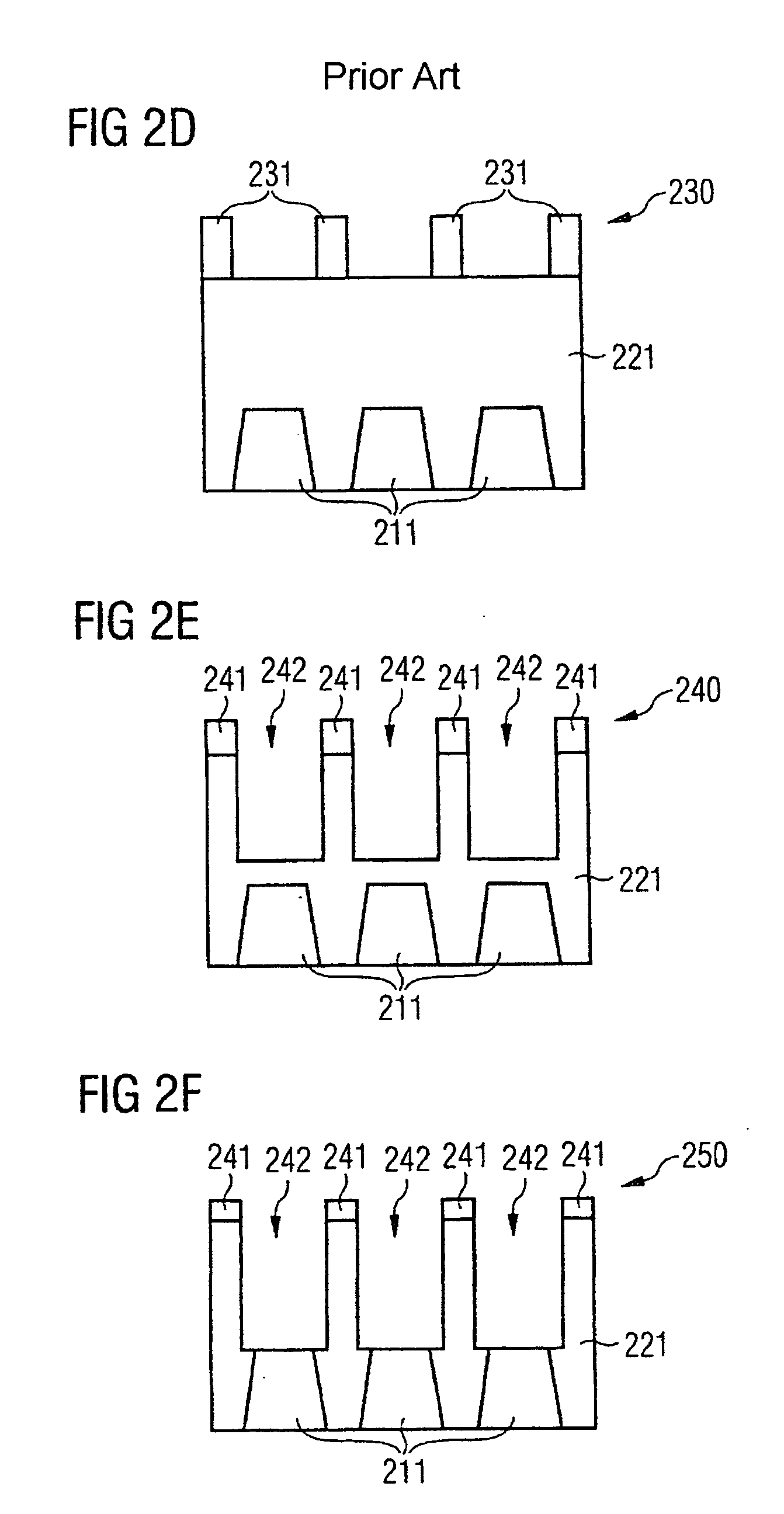
During etching of the electrically insulating layer according to the prior art, the problem occurs that the thickness of the electrically insulating layer is frequently relatively large and different for different individual areas of the patterned electrically conductive layer which, for reliably exposing all individual areas, requires an extended etching time which can lead to formation of unwanted narrow gaps in some of the individual areas (see FIG. 2E to FIG. 2H).

Method used


Image

  • Method for producing a layer arrangement
  • Method for producing a layer arrangement
  • Method for producing a layer arrangement

Examples


Embodiment Construction

[0069]In the further text, a method for producing a layer arrangement according to a first exemplary embodiment of the invention is described with reference to FIG. 3A to FIG. 3H.

[0070]To obtain the layer sequence 300 shown in FIG. 3A, an aluminum layer 301 is formed on a silicon substrate (not shown) by using a conformal deposition process. On the aluminum layer 301, a silicon nitride sacrificial layer 302 is deposited conformally by using a CVD process. As an alternative, such a sacrificial layer can also be formed of silicon oxynitride material. On the silicon nitride sacrificial layer 302, photoresist material is formed and patterned to form a photoresist mask 303 by using a lithography process and an etching process.

[0071]To obtain the layer sequence 310 shown in FIG. 3B, the aluminum layer 301 and the silicon nitride sacrificial layer 302, starting from the layer sequence 300 shown in FIG. 3A, are patterned jointly, i.e. in an associated method step, by using an etching proces...


PUM


Abstract

The invention relates to a method for producing a layer arrangement. An electrically conductive layer is formed and patterned. A sacrificial layer formed on at least part of the patterned electrically conductive layer. An electrically insulating layer is formed on the electrically conductive and sacrificial layers and is patterned in such a manner that one or more surface areas of the sacrificial layer are exposed. The exposed areas of the sacrificial layer are removed to expose one or more surface areas of the patterned electrically conductive layer. The patterned electrically conductive layer is covered with a pattern of electrically conductive material.

Description

PRIORITY CLAIM[0001]This application is a national stage application of international application number PCT / DE2005 / 001067, filed on Jun. 15, 2005, which claims the benefit of priority to German Patent Application DE 10 2004 029 519.0, filed Jun. 18, 2004, which are incorporated herein by reference.TECHNICAL FIELD[0002]The invention relates to a method for manufacturing a layer arrangement.BACKGROUND INFORMATION[0003]In integrated circuits, a vertical electrical contact is established between conductor tracks of different metallization levels by using so-called vias. Vias, i.e. trenches orientated vertically with respect to a substrate surface, are frequently created by using a lithography and a plasma etching method and can then be filled with electrically conductive material. Between the material of a conductor track of a metallization level to be contacted, and the material of a via, an adhesive, barrier or seed layer (liner layer) can be provided by means of which a contact can ...

Claims


Application Information

Patent Timeline
Patent Type & Authority Applications(United States)
IPC IPC(8): H01L21/4763H01L21/768
CPCH01L21/76834H01L21/76802
Inventor ECKERT, STEFANGOLLER, KLAUSWENDT, HERMANN
Owner INFINEON TECH AG
Why Eureka
Try Eureka