Method Of Attaching A Solder Element To Contact And The Contact Assembly Formed Thereby

a technology of contact and solder element, which is applied in the direction of soldering apparatus, sustainable manufacturing/processing, final product manufacturing, etc., can solve the problems of difficult maintenance of the co-planarity of the ball grid array with the conductive pads on the printed wiring board, and the difficulty of assembly of the solder ball

Active Publication Date: 2008-05-08
MOLEX INC
View PDF26 Cites 20 Cited by
  • Summary
  • Abstract
  • Description
  • Claims
  • Application Information

AI Technical Summary

Problems solved by technology

The solder balls can be difficult to assemble with the contacts as they are loose.
In addition, the assembly of the solder ball is fragile (balls may fall off).
Furthermore, the co-planarity of the ball grid array with the conductive pads on the printed wiring board can be difficult to maintain because each ball sits on top of the solder paste on the conductive pad of the printed wiring board and the solder ball can interfere with the co-planarity of the contact field between the contact and the conductive pad.
Additionally, when the solder ball is melted to form a solder joint between the contact and the conductive pad, a bulge may form.
This bulge in the solder joint can cause shorts between adjacent contacts.

Method used


Image

  • Method Of Attaching A Solder Element To Contact And The Contact Assembly Formed Thereby
  • Method Of Attaching A Solder Element To Contact And The Contact Assembly Formed Thereby
  • Method Of Attaching A Solder Element To Contact And The Contact Assembly Formed Thereby

Examples


first embodiment

[0034]Attention is now invited to the invention shown in FIGS. 1-6.

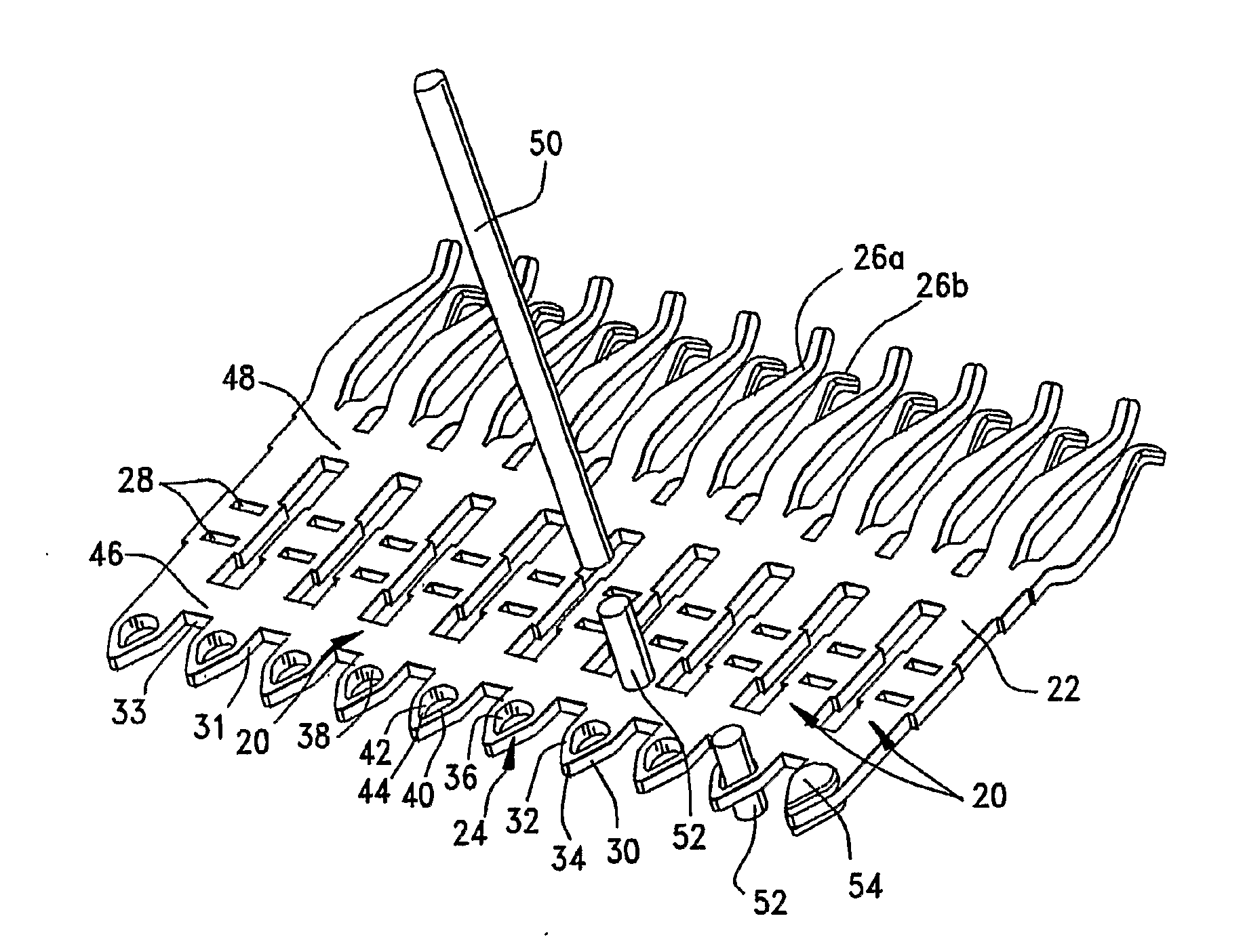
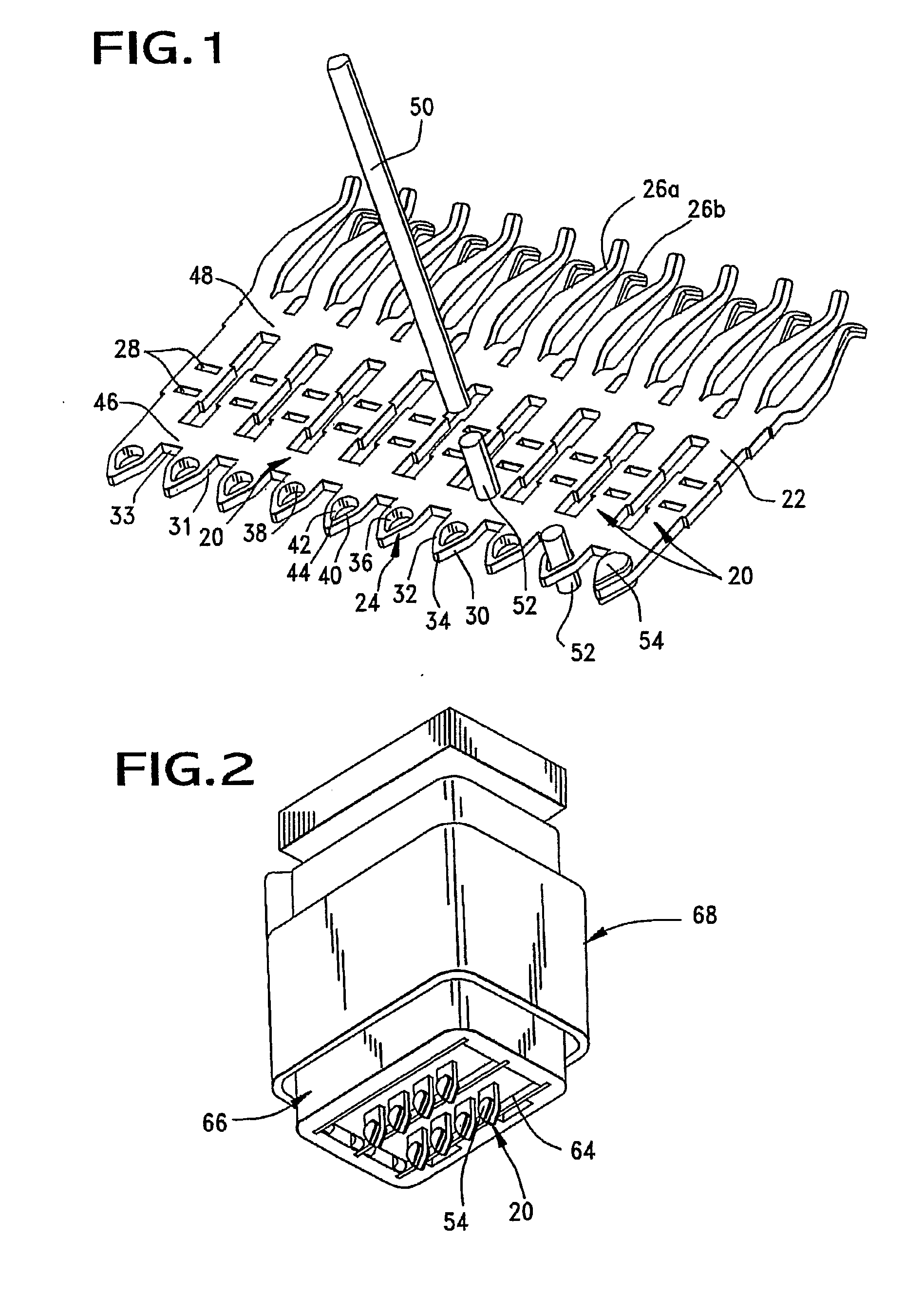
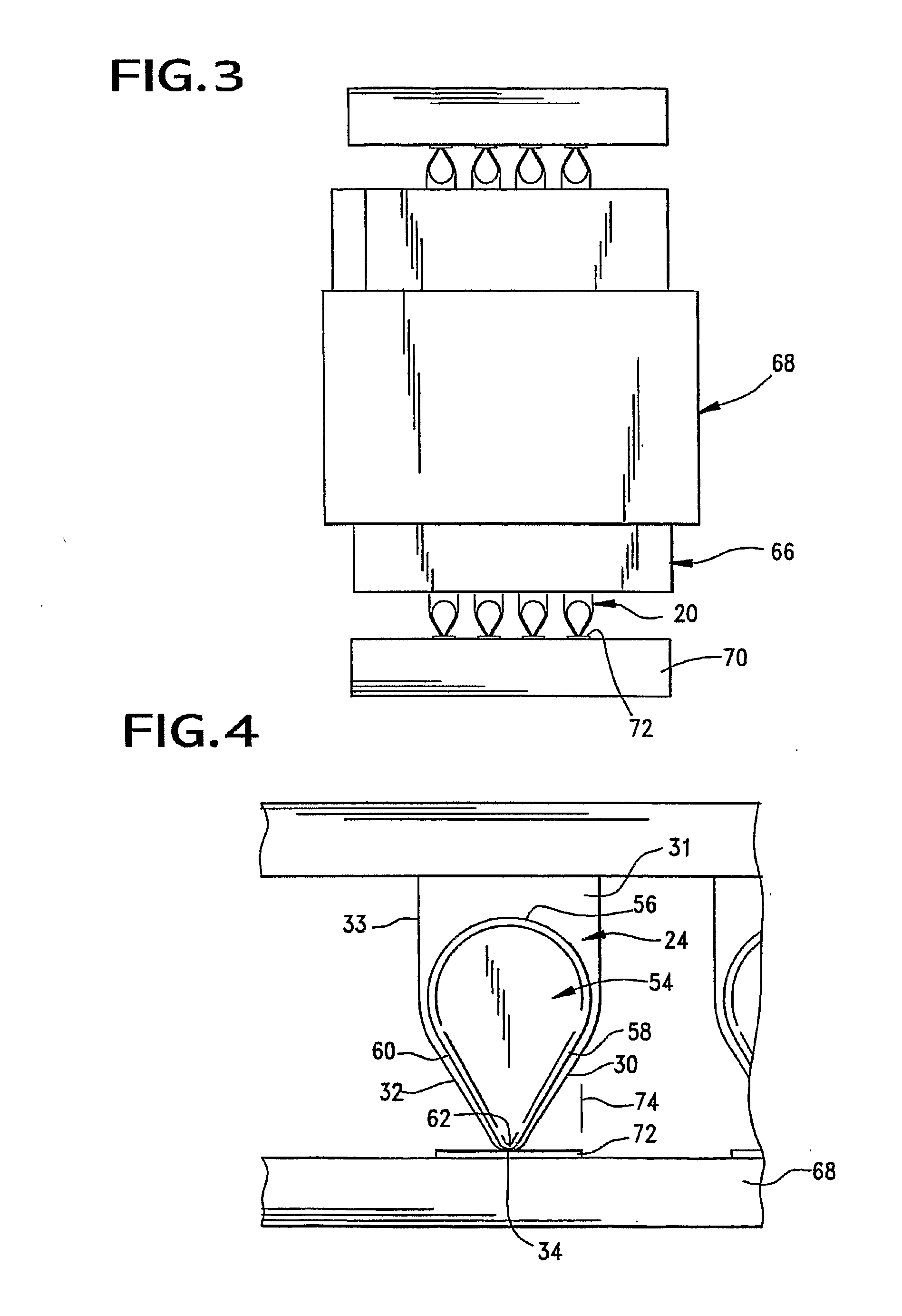
[0035]Initially, a sheet of conductive material (not shown) is provided. A continuous strip of contacts 20 is formed out of the sheet material by conventional means, such as stamping and forming the contacts 20 out of the sheet. Each contact 20 includes generally rectangular body 22 having a tail 24 at first end thereof and a pair of mating contacts 26a, 26b at the second end thereof. The body 22 has a pair of apertures 28 therethrough for attachment of the respective contact 20 to a wafer. The tail 24 of each contact 20 is generally shaped like a “tear-drop”. The tail 24 includes straight sides 31, 33 which are parallel to the sides of the body 22 and sides 30, 32 that extend therefrom and taper inwardly to a rounded point 34. An aperture 36 is provided through the tail 24. The aperture 36 is generally shaped like a “tear-drop” such that the base 38 of the aperture 36 is round and the sides 40, 42 of the aperture 36...

second embodiment

[0045]Attention is now invited to the invention shown in FIGS. 7-13.

[0046]Initially, a sheet of conductive material (not shown) is provided. A continuous strip of contacts 120 is formed out of the sheet material by conventional means, such as stamping the contacts 120 out of the sheet. Each contact 120 includes a generally rectangular body 122 having a tail 124 at first end thereof and a mating contact 126 at the second end thereof. While a male contact 120 is shown in the second embodiment, it is to be understood that a female contact can be formed by forming an appropriate female mating contact. The body 122 has an aperture 128 therethrough for attachment of the respective contact 120 to a wafer 164. The tail 124 of each contact 120 is generally shaped like a “wolf head”. The tail 120 has straight side edges 131, 133 which are parallel to the side edges of the rectangular body 122. A bottom edge has generally flat end sections 130, 132 with a curved intermediate section 134 thereb...

sixth embodiment

[0079]Attention is now invited to the invention shown in FIGS. 20-23.

[0080]Initially, a sheet of conductive material (not shown) is provided. A continuous strip of contacts 520 is formed out of the sheet material by conventional means, such as stamping and forming the contacts 520 out of the sheet. Each contact 520 includes generally rectangular body 522 having a tail 524 at first end thereof and a mating contact 526 at the second end thereof. The body 522 has a pair of apertures 528 therethrough for attachment of the respective contact 520 to a wafer. The tail 524 of each contact 520 is generally rounded. The tail 524 includes straight sides 531, 533 which are parallel to the sides of the body 522 and a rounded end 534. An aperture 536 is provided through the tail 524. The aperture 536 is generally round, but other shapes may be provided. The mating contact 526 is conventional and allow for a mating contact (not shown) to be inserted therebetween. While a male contact 520 is shown ...


PUM

PropertyMeasurementUnit
shapeaaaaaaaaaa
conductiveaaaaaaaaaa
shapesaaaaaaaaaa

Abstract

A method of attaching a solder element to a contact and the contact assembly formed thereby. The contact assembly is used in a connector. The solder element is either staked or stapled to the contact. The solder element can take a variety of shapes and disclosed herein is a tear-drop shape, a “wolf's head” shape and a circular shape. An over-stress feature is also provided for when the contact assembly is mounted to a printed wiring board.

Description

[0001]This application claims the benefit of U.S. provisional application Ser. No. 60 / 610,069, filed on Sep. 15, 2004 and herein incorporates same by reference.BACKGROUND OF THE INVENTION[0002]In prior art methods of assembling a ball grid array, a solder ball is fused to the end of a contact. The solder balls can be difficult to assemble with the contacts as they are loose. In addition, the assembly of the solder ball is fragile (balls may fall off). Furthermore, the co-planarity of the ball grid array with the conductive pads on the printed wiring board can be difficult to maintain because each ball sits on top of the solder paste on the conductive pad of the printed wiring board and the solder ball can interfere with the co-planarity of the contact field between the contact and the conductive pad. Additionally, when the solder ball is melted to form a solder joint between the contact and the conductive pad, a bulge may form. This bulge in the solder joint can cause shorts between...

Claims


Application Information

Patent Timeline
Patent Type & Authority Applications(United States)
IPC IPC(8): H05K3/34B23K20/02B23K31/00H01R12/55
CPCB23K1/0008B23K2201/36H01R4/02H01R43/0235H05K2203/0415H01R43/16H05K3/3426H05K2201/10984H01R43/0256B23K2101/36Y02P70/50
Inventor PELOZA, KIRK B.FAJE, RICHARD A.HODGE, RONALD C.GOULD, JOS S.
Owner MOLEX INC
Why Eureka
Try Eureka