Emitter Ballasting by Contact Area Segmentation in ESD Bipolar Based Semiconductor Component

a bipolar based semiconductor and contact area segmentation technology, applied in the field of integrated circuits, can solve the problems of esd electrical currents, ics pose a significant danger, and the gap between esd and ics to become electrically conducting, and achieve the effects of high electrical currents, high currents, and high currents

Active Publication Date: 2008-07-17
TEXAS INSTR INC
View PDF8 Cites 9 Cited by
  • Summary
  • Abstract
  • Description
  • Claims
  • Application Information

AI Technical Summary

Problems solved by technology

These features of electrical environments, especially charge sources, pose a significant danger to ICs.
When charge sources come into close proximity to ICs, large potential differences between charge sources and ICs, typically between a few tens of volts and a few thousand volts, can cause a gap between them to become electrically conducting as a result of avalanche ionization and breakdown of a separating medium, usually air.
Electrical currents associated with ESD are typically very high and can damage components of an IC.
Nevertheless, ICs are subject to ESD incidents.
Current inhomogeneity and current crowding are well known to be issues in bipolar transistors in ESD protection circuits.
Current crowding occurring during ESD events can result in permanent damage to bipolar transistors, causing loss of circuit functionality or shortened operating life of ESD protection circuit and IC.

Method used


Image

  • Emitter Ballasting by Contact Area Segmentation in ESD Bipolar Based Semiconductor Component
  • Emitter Ballasting by Contact Area Segmentation in ESD Bipolar Based Semiconductor Component
  • Emitter Ballasting by Contact Area Segmentation in ESD Bipolar Based Semiconductor Component

Examples


Embodiment Construction

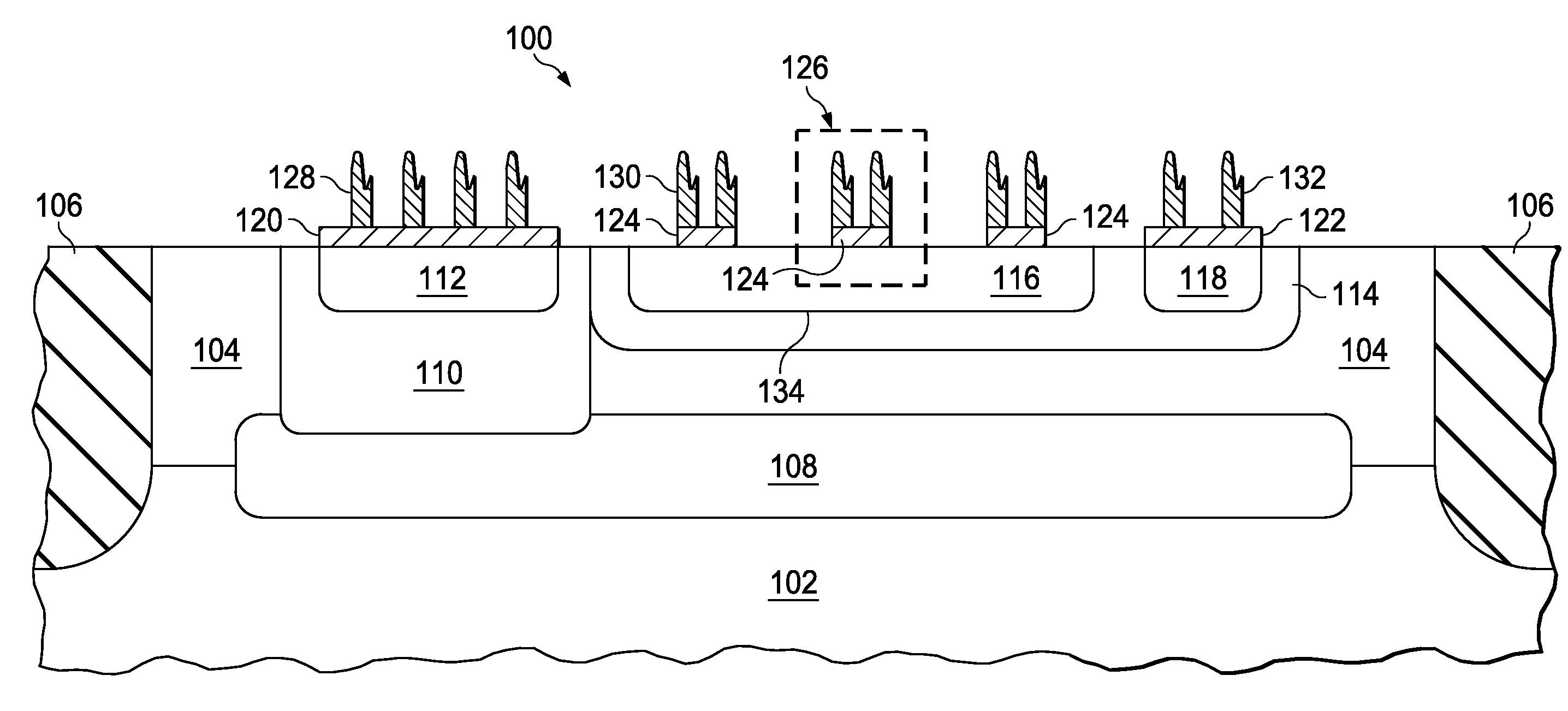
[0014]For the purposes of this disclosure, a contact island is defined as a region containing a plurality of contacts wherein said contacts are spaced more closely to one another than to other contacts not in said contact island. If metal silicide is used in said contact island, the contact island extends to the boundaries of the metal silicide.

[0015]For the purposes of this disclosure, an emitter diffused region is defined as a contiguous region of IC substrate forming part or all of an emitter of a bipolar transistor, in which said contiguous region of IC substrate is doped the same type throughout. The boundary of said emitter diffused region extends to the boundary of the contiguous region of IC substrate with the same type doping as said emitter diffused region.

[0016]FIG. 1 is a cross-section of a bipolar transistor with multiple emitter contact islands according to an embodiment of the instant invention. An IC (100) includes a substrate (102), which may have an epitaxial layer...


PUM


Abstract

Integrated circuits (ICs) utilize bipolar transistors in electro-static discharge (ESD) protection circuits to shunt discharge currents during ESD events to protect the components in the ICs. Bipolar transistors are subject to non-uniform current crowding across the emitter-base junction during ESD events, which results in less protection for the IC components and degradation of the bipolar transistor. This invention comprises multiple contact islands (126) on the emitter (116) of a bipolar transistor, which act to spread current uniformly across the emitter-base junction. Also included in this invention is segmentation of the emitter diffused region to further improve current uniformity and biasing of the transistor. This invention can be combined with drift region ballasting or back-end ballasting to optimize an ESD protection circuit.

Description

FIELD OF THE INVENTION[0001]This invention relates to the field of integrated circuits. More particularly, this invention relates to bipolar transistors as independent components and as elements of electronic components in integrated circuits.BACKGROUND OF THE INVENTION[0002]It is well known that integrated circuits (ICs) are comprised of microelectronic components such as transistors, diodes, resistors, capacitors, etc., in a substrate, and metal interconnects which connect the components in circuits. It is furthermore well known that some internal nodes of an IC are connected to external nodes. Internal nodes of an IC are connected to external nodes by metal elements, known as Input-Output (IO) pads or bondpads, among other designations, on the top surface of an IC. IO pads are connected to external functions by various means, including wirebonding, bumpbonding, beamlead bonding, etc. By necessity, internal nodes of an IC that are connected to IO pads are exposed to the electrical...

Claims


Application Information

Patent Timeline
Patent Type & Authority Applications(United States)
IPC IPC(8): H01L27/102H01L21/8249
CPCH01L27/0259H01L27/0641H01L24/05H01L2924/13091H01L2924/1305H01L2924/00H01L2924/14
Inventor DENISON, MARIE
Owner TEXAS INSTR INC
Why Eureka
Try Eureka