Atomic layer deposition systems and methods

a technology of atomic layer and thin film, applied in chemical vapor deposition coating, coating, metallic material coating process, etc., can solve the problems of significant reduction of commercial value, process chamber purged, and thin film purity dwindling

Active Publication Date: 2008-08-14
TOKYO ELECTRON LTD
View PDF33 Cites 332 Cited by
  • Summary
  • Abstract
  • Description
  • Claims
  • Application Information

AI Technical Summary

Problems solved by technology

Additionally, CVD tends to incorporate undesired reaction products into the deposited thin film, thereby diminishing the purity of the thin film.
Nevertheless, a major disadvantage of a single wafer reactor is that it has a significantly diminished commercial value because of its relatively low throughput.
Another disadvantage is that the process chamber must be purged before each individual gas precursor is introduced.
One characteristic disadvantage of these multi-wafer reactors is that multi-wafer reactors employ showerhead injectors that inject the precursor gases in an axially symmetric direction generally perpendicular to the substrate surface.
As a result, although faster process times are achieved, multi-wafer ALD process chambers may produce thin films with reduced thickness uniformity.

Method used


Image

  • Atomic layer deposition systems and methods
  • Atomic layer deposition systems and methods
  • Atomic layer deposition systems and methods

Examples


Embodiment Construction

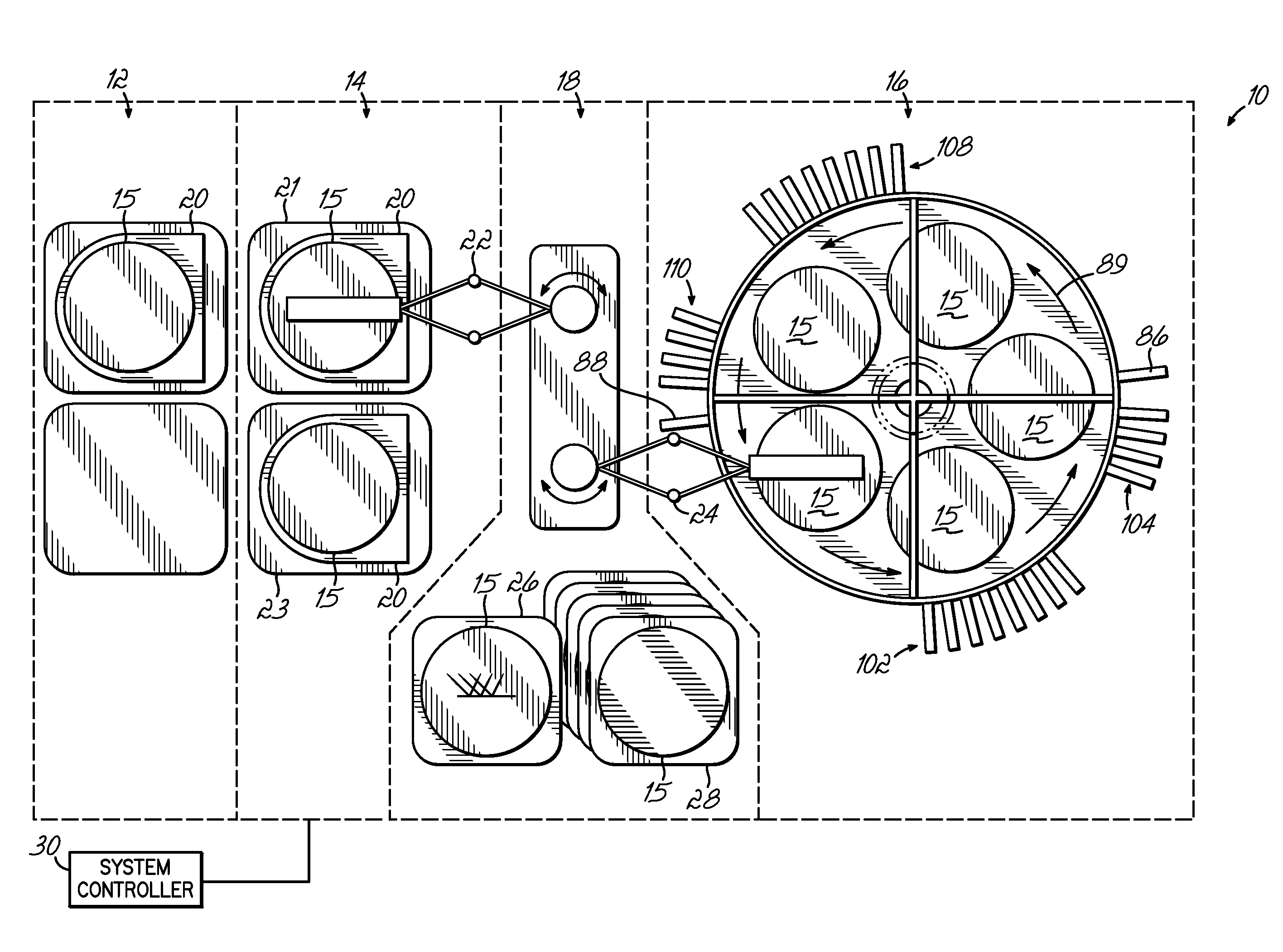
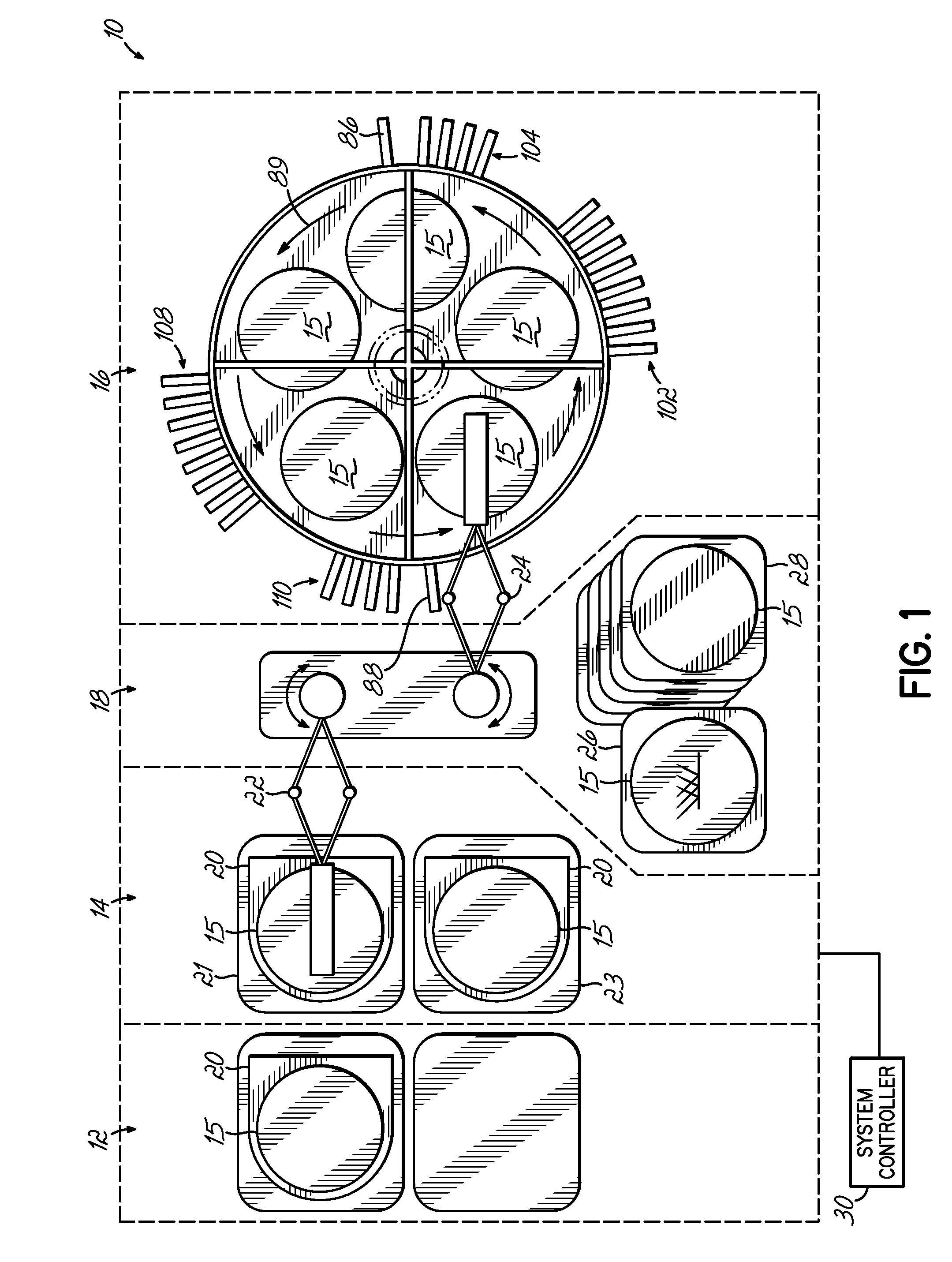
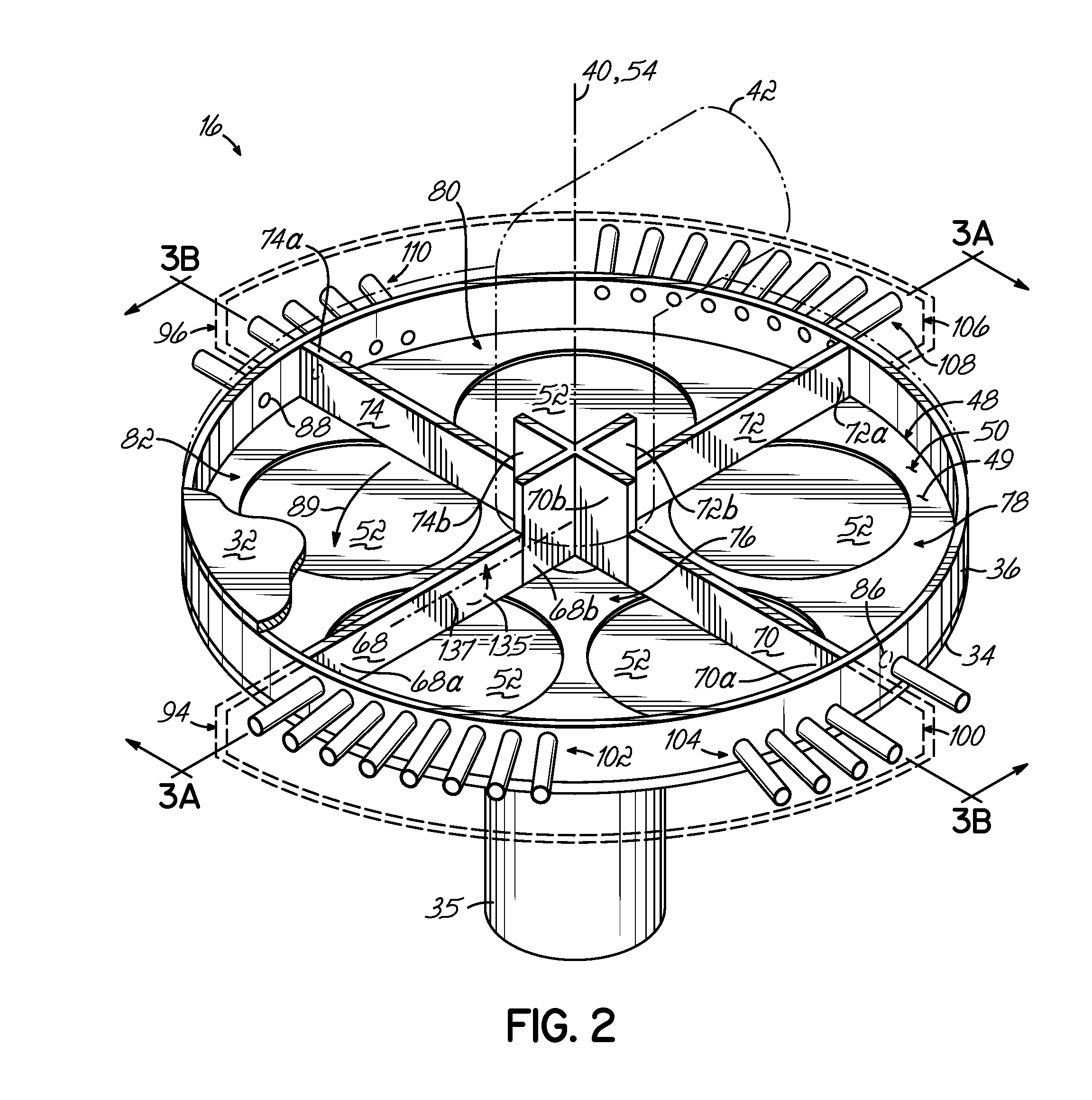
[0020]With reference to FIG. 1, a deposition system 10 for processing a plurality of substrates 15 comprises an input / output station 12, a load / lock station 14, a process chamber 16, and a transfer chamber 18 interposed between the load / lock station 14 and process chamber 16. The deposition system 10, which is shown in a simplified manner, may include additional structures, such as additional vacuum-isolation walls coupling the load / lock station 14 with the transfer chamber 18 and the process chamber 16 with the transfer chamber 18, as understood by a person having ordinary skill in the art. The input / output station 12, which is at or near atmospheric pressure (e.g., 760 Torr), is adapted to receive wafer cassettes 20, such as front opening unified pods (FOUPs). The wafer cassettes 20 are sized and shaped to hold a plurality of substrates 15, such as semiconductor wafers having diameters of, for example, 200 or 300 millimeters.

[0021]The load / lock station 14 is adapted to be evacuate...


PUM

PropertyMeasurementUnit
atmospheric pressureaaaaaaaaaa
diametersaaaaaaaaaa
diametersaaaaaaaaaa

Abstract

Systems and methods for depositing thin films using Atomic Layer Deposition (ALD). The deposition system includes a process chamber with a peripheral sidewall, partitions that divide a processing space inside the process chamber into at least first and second compartments, and a platter that supports substrates within the processing space. The platter rotates the substrates relative to the stationary peripheral sidewall and compartments. The first compartment receives a process material used to deposit a layer on each of the substrates. An injector, which injects the process material, communicates with the first compartment through the peripheral sidewall.

Description

FIELD OF THE INVENTION[0001]This invention relates to systems and methods for depositing thin films using Atomic Layer Deposition (ALD).BACKGROUND OF THE INVENTION[0002]As dimensions for microelectronics are reduced and the demand for such materials increase, thin semiconductor films having uniform composition and uniform thickness over a larger substrate area are increasingly desirable. A common process used for depositing thin films on a substrate is Chemical Vapor Deposition (CVD), which provides for deposition of relatively uniform films over complex device topography. In a typical CVD process, the substrate is exposed to two or more volatile precursors, which react and / or decompose on the substrate surface to produce the desired thin film.[0003]Despite improvements of CVD over previous deposition techniques, CVD has several disadvantages. For example, because CVD is flux-dependent, deposition conditions such as substrate temperature, pressure, and gas flow rate must be accurate...

Claims


Application Information

Patent Timeline
Patent Type & Authority Applications(United States)
IPC IPC(8): C23C16/00
CPCC23C16/45508C23C16/45519C23C16/45536H01L21/68771C23C16/4584C23C16/54H01L21/68764C23C16/45551C23C16/45525H01L21/0262
Inventor DIP, ANTHONY
Owner TOKYO ELECTRON LTD
Why Eureka
Try Eureka