Multilayer electronic component and method for manufacturing the same

a technology of electronic components and manufacturing methods, applied in the direction of fixed capacitor details, stacked capacitors, fixed capacitors, etc., can solve the problems of reducing the life affecting the performance of multi-layer electronic components, and disadvantageous entry of moisture and other contaminants

Active Publication Date: 2008-09-04
MURATA MFG CO LTD
View PDF20 Cites 61 Cited by
  • Summary
  • Abstract
  • Description
  • Claims
  • Application Information

AI Technical Summary

Benefits of technology

[0010]To overcome the problems described above, preferred embodiments of the present invention provide a method for manufacturing a multilayer electronic component, and a multilayer electronic component manufactured thereby.

Problems solved by technology

However, in the method disclosed in Japanese Unexamined Patent Application Publication No. 63-169014, since the bonding between the internal electrodes and the plating film is insufficient, moisture and other contaminants are disadvantageously likely to enter the laminate.
Thus, when a loading test is performed under high-temperature and high-humidity conditions, the life of a multilayer electronic component is likely to be reduced.

Method used


Image

  • Multilayer electronic component and method for manufacturing the same
  • Multilayer electronic component and method for manufacturing the same
  • Multilayer electronic component and method for manufacturing the same

Examples


Embodiment Construction

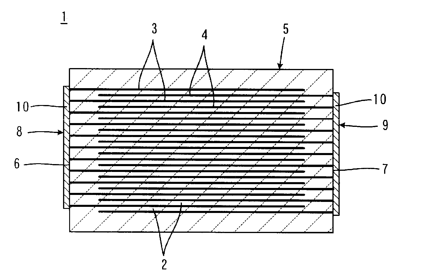
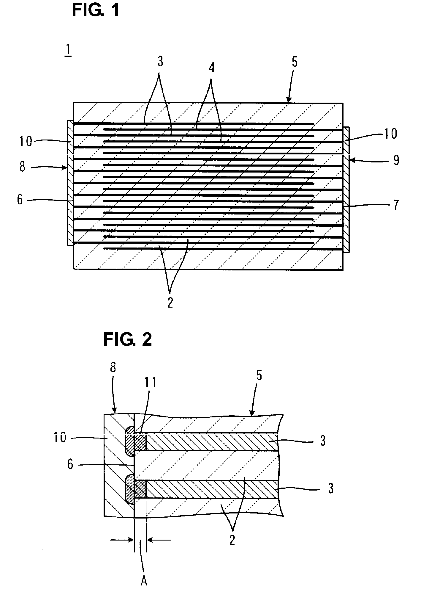
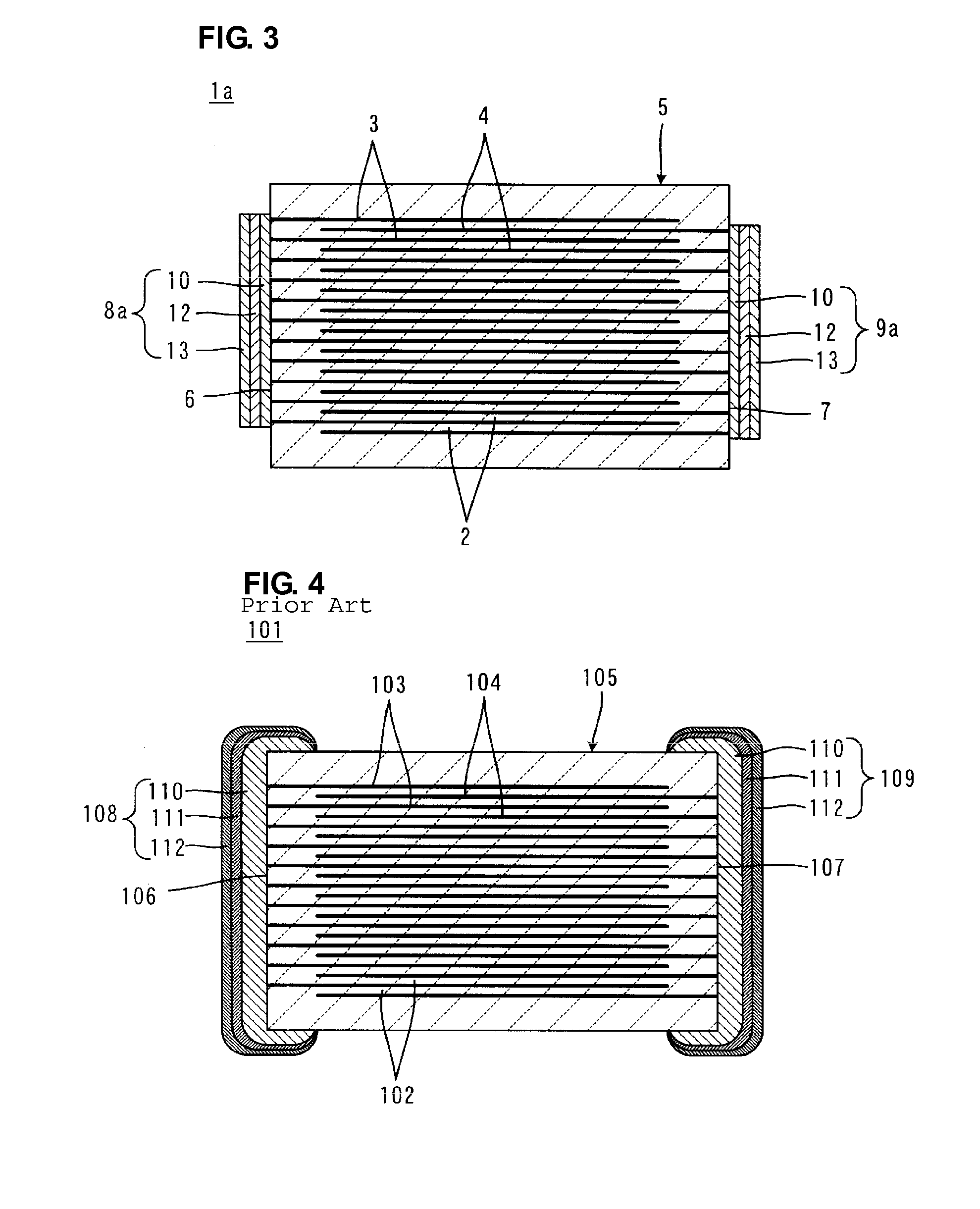
[0029]With reference to FIGS. 1 and 2, a multilayer electronic component 1 according to a first preferred embodiment of the present invention and a method for manufacturing the same will be described.

[0030]First, as shown in FIG. 1, the multilayer electronic component 1 includes a laminate 5 which includes a plurality of insulating layers 2 laminated to each other and layer-shaped internal electrodes 3 and 4 provided along interfaces between the insulating layers 2. When the multilayer electronic component 1 is a multilayer ceramic capacitor, the insulating layers 2 are made of a dielectric ceramic. At end surfaces 6 and 7 of the laminate 5, edges of a plurality of internal electrodes 3 and 4 are exposed, respectively, and external electrodes 8 and 9 are provided so as to electrically connect the edges of the internal electrodes 3 and the edges of the internal electrodes 4, respectively.

[0031]Each of the external electrodes 8 and 9 are defined by a plating film 10 of plating deposit...


PUM

PropertyMeasurementUnit
temperatureaaaaaaaaaa
thicknessaaaaaaaaaa

Abstract

A method for manufacturing a multilayer electronic component, includes the steps of preparing a laminate including a plurality of insulating layers laminated to each other and a plurality of internal electrodes formed along interfaces between the insulating layers, edges of the internal electrodes being exposed at a predetermined surface of the laminate, and forming an external electrode on the predetermined surface so as to electrically connect the edges of the internal electrodes, which are exposed at the predetermined surface of the laminate. The step of forming an external electrode includes a plating step of forming a continuous plating film by depositing plating deposits on the edges of the internal electrodes exposed at the predetermined surface of the laminate which is prepared in the step of preparing a laminate and by performing plating growth of the plating deposits so as to be connected to each other, and a heat treatment step of performing a heat treatment on the laminate provided with the plating film formed thereon at an oxygen partial pressure of about 5 ppm or less and at a temperature of about 600° C. or more.

Description

BACKGROUND OF THE INVENTION[0001]1. Field of the Invention[0002]The present invention relates to a multilayer electronic component and a method for manufacturing the same, and more particularly to a multilayer electronic component formed by plating external electrodes directly on external surfaces of a laminate and to a method for manufacturing the multilayer electronic component.[0003]2. Description of the Related Art[0004]As shown in FIG. 4, a multilayer electronic component 101, which is represented by a multilayer ceramic capacitor, generally includes a laminate 105 including a plurality of insulating layers 102 laminated to each other and a plurality of layer-shaped internal electrodes 103 and 104 provided along interfaces between the insulating layers 102. At end surfaces 106 and 107 of the laminate 105, edges of the internal electrodes 103 and 104 are exposed, respectively, and external electrodes 108 and 109 are provided to electrically connect the edges of the internal elec...

Claims


Application Information

Patent Timeline
Patent Type & Authority Applications(United States)
IPC IPC(8): C25D5/02H01G4/008
CPCH01G4/012H01G4/2325H01G4/30H01L41/083H01G4/308H01C7/008H01F27/2804B05D5/12H01G4/228H01G4/005H10N30/50
Inventor MOTOKI, AKIHIROOGAWA, MAKOTOKAWASAKI, KENICHITAKEUCHI, SHUNSUKEKURODA, SHIGEYUKI
Owner MURATA MFG CO LTD
Why Eureka
Try Eureka