
Eureka
For R&D, Eureka makes reading and utilizing patents & technical documents easy.
Eureka AIR
Designed for self-driven R&D workflows. Generate viable solutions, solve complex R&D challenges, empower your innovation with AI.

Eureka Materials
Designed for material experts only. Revolutionize your material R&D, from search, analyze, to developing new materials.

TechResearch
Generate reliable direction feasibility study reports for your R&D in just a few steps.

TechSeek
Discover and master advanced knowledge NOW. Basics, ideas, possibilities, all at once.

TechMind
As an expert in R&D Theories, TechMind can generates customized viable solutions instantly.

TechRisk
Analyze your overall solution with one click, know your potential R&D risks in advance.

TechMonitor
Get weekly tech updates, stay abreast of the latest tech innovations and key insights.
Semiconductor device and manufacturing method thereof
- Summary
- Abstract
- Description
- Claims
- Application Information
AI Technical Summary
Problems solved by technology
Method used
Image

Examples
first embodiment
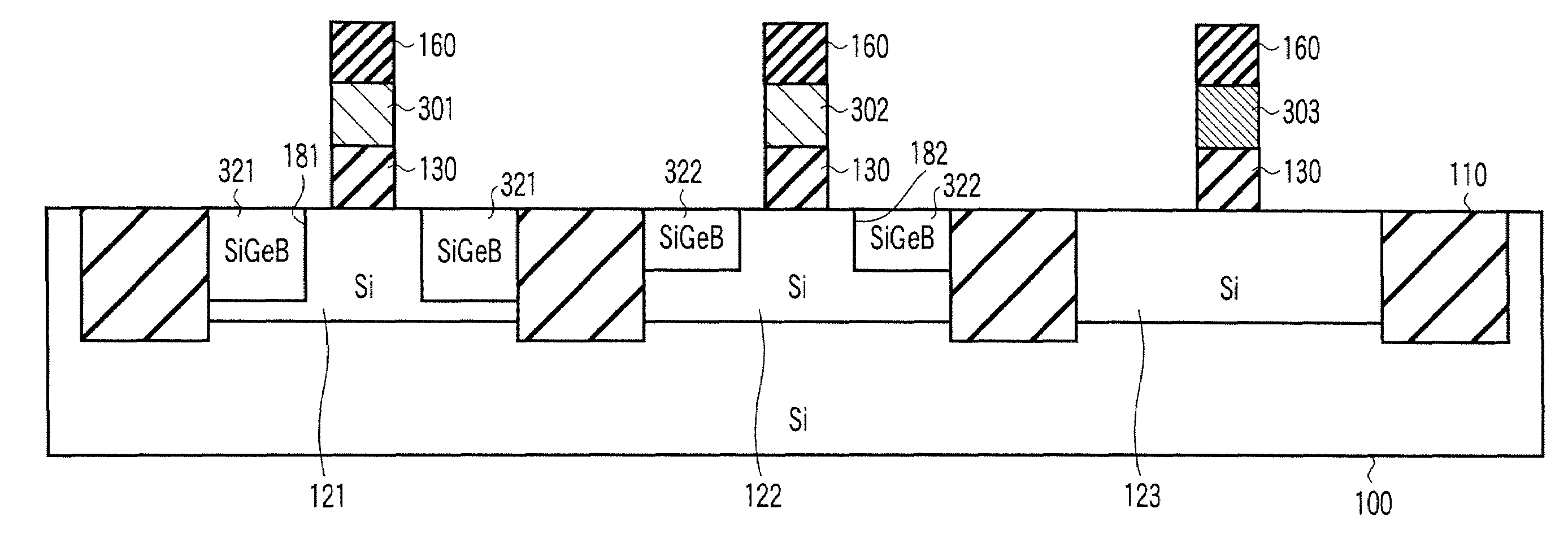
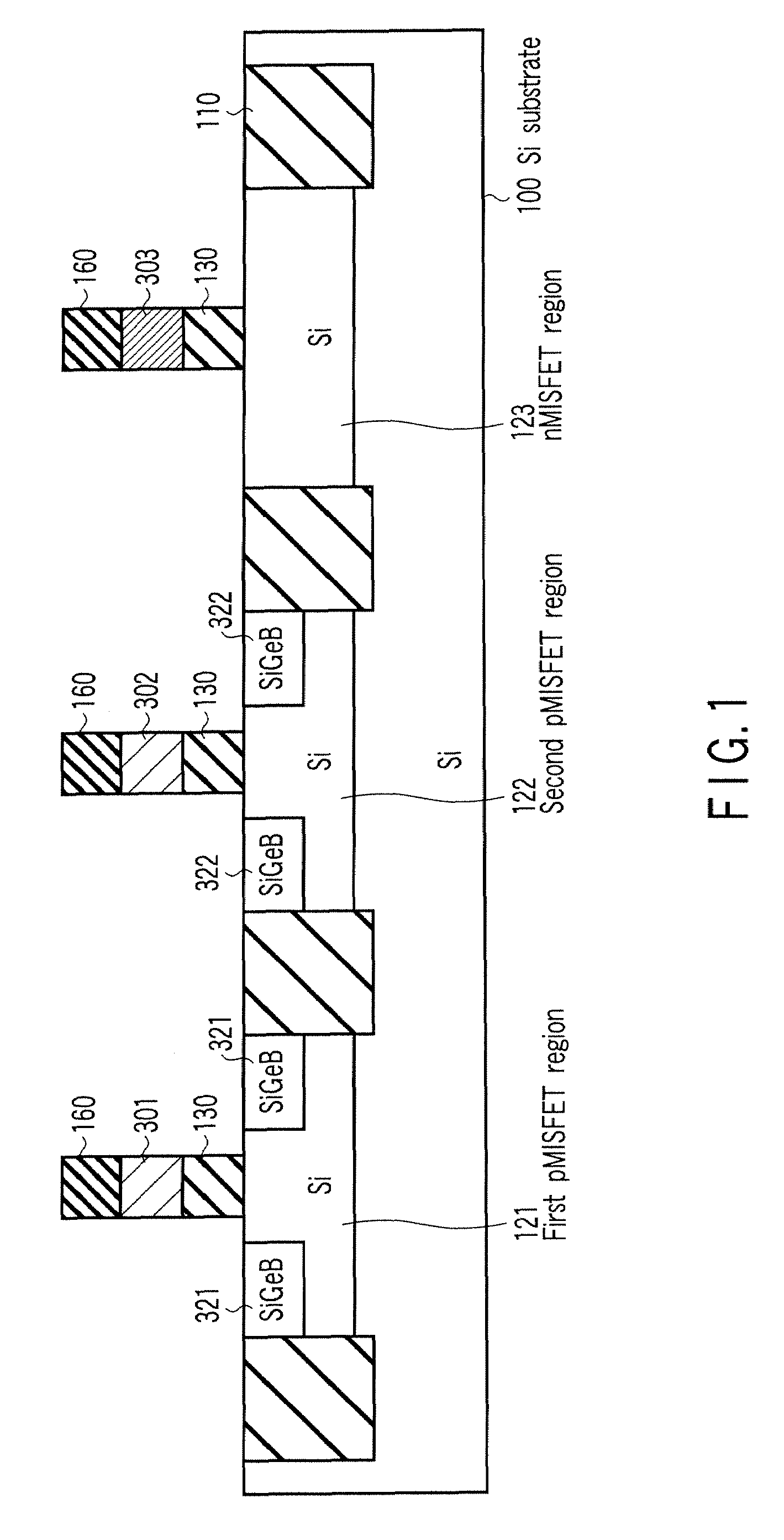
[0022]FIG. 1 is a cross-sectional view showing the schematic structure of a semiconductor device according to a first embodiment of this invention.
[0023]An element isolation insulating film 110 is formed on a surface portion (well) of an Si substrate 100 and a first pMISFET region 121, second pMISFET region 122 and nMISFET region 123 are formed in portions surrounded by the element isolation insulating film 110. A gate electrode 301 is formed above the pMISFET region 121 with a gate insulating film 130 disposed therebetween and source / drain regions are formed with the gate electrode 301 used as a mask so as to form a first p-channel MIS transistor. A gate electrode 302 is formed above the pMISFET region 122 with a gate insulating film 130 disposed therebetween and source / drain regions are formed with the gate electrode 302 used as a mask so as to form a second p-channel MIS transistor. Further, a gate electrode 303 is formed above the nMISFET region 123 with a gate insulating film 1...
second embodiment
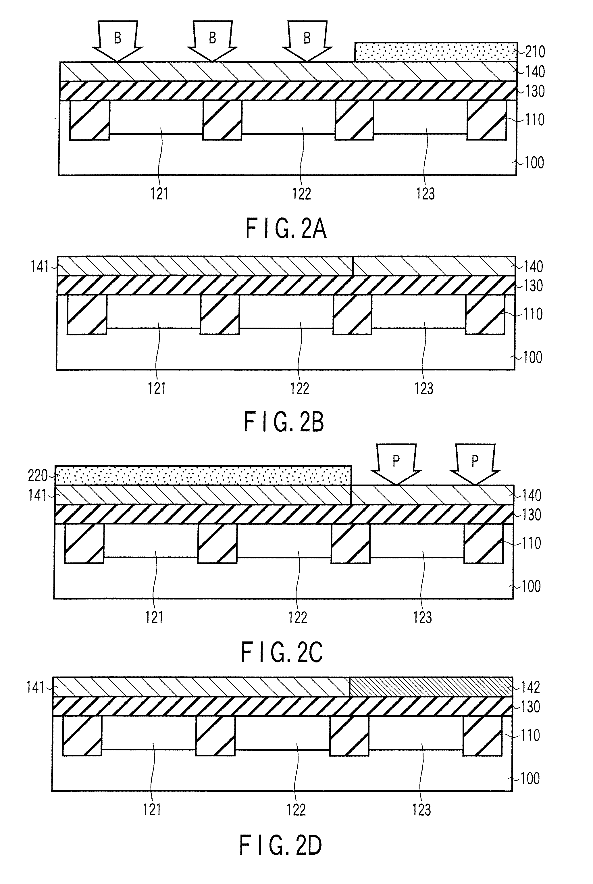
[0048]FIG. 4 is a cross-sectional view showing the schematic structure of a semiconductor device according to a second embodiment of this invention. The same symbols are attached to the same portions as those of FIG. 1 and the detail explanation thereof is omitted.
[0049]The present embodiment is different from the first embodiment in that the areas of element isolation insulating films in the respective pMISFET regions are made different in order to change the Ge concentrations in the SiGe films. That is, as shown in FIGS. 5A and 5B, the areas of element isolation insulating films 110 in a first pMISFET region 121 and second pMISFET region 122 are made different. The area of the element isolation insulating film 110 is made larger in the first pMISFET region 121, and as a result, the area of the first pMISFET region 121 is made smaller than that of the second pMISFET region 122.
[0050]In this case, in one cell region containing a MISFET region and element isolation region, the ratio ...
PUM
 Abstract
Description
Claims
Application Information
 - R&D Engineer
- R&D Manager
- IP Professional
- Industry Leading Data Capabilities
- Powerful AI technology
- Patent DNA Extraction
Browse by: Latest US Patents, China's latest patents, Technical Efficacy Thesaurus, Application Domain, Technology Topic, Popular Technical Reports.
© 2024 PatSnap. All rights reserved.Legal|Privacy policy|Modern Slavery Act Transparency Statement|Sitemap|About US| Contact US: help@patsnap.com