Stacked electronic component package having single-sided film spacer

a technology of electronic components and film spacers, which is applied in the direction of electrical equipment, semiconductor devices, semiconductor/solid-state device details, etc., can solve the problems of reducing the yield affecting the yield of electronic components, and adhesion of the upper surface of double-sided film spacers, etc., to achieve the effect of minimizing the yield of fabrication of stacked electronic component packages and minimal costs

Inactive Publication Date: 2008-10-02
AMKOR TECH INC DW US
View PDF92 Cites 19 Cited by
  • Summary
  • Abstract
  • Description
  • Claims
  • Application Information

AI Technical Summary

Benefits of technology

[0012]An upper surface of a film, e.g., an organic film, of the single-sided film spacer is nonadhesive. Accordingly, the single-sided film spacer does not stick to the pickup tool during retraction of the pickup tool from the single-sided film spacer. Thus, voiding between the single-sided film spacer and ...

Problems solved by technology

One problem associated with the double-sided film spacer was that the adhesive upper surface of the double-sided film spacer adhered to the vacuum head of the pickup tool.
Thus, during retraction of the vacuum head, the double-sided film spacer was pulled from the upper surface of the lower electronic component resulting in the formation of interfacial voids...

Method used


Image

  • Stacked electronic component package having single-sided film spacer
  • Stacked electronic component package having single-sided film spacer
  • Stacked electronic component package having single-sided film spacer

Examples


Embodiment Construction

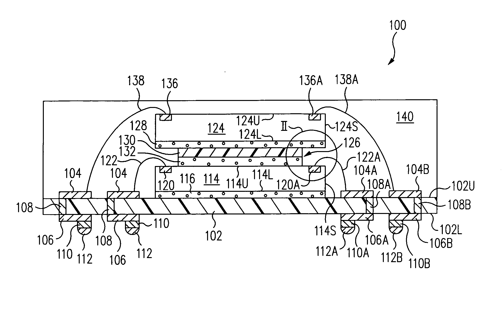
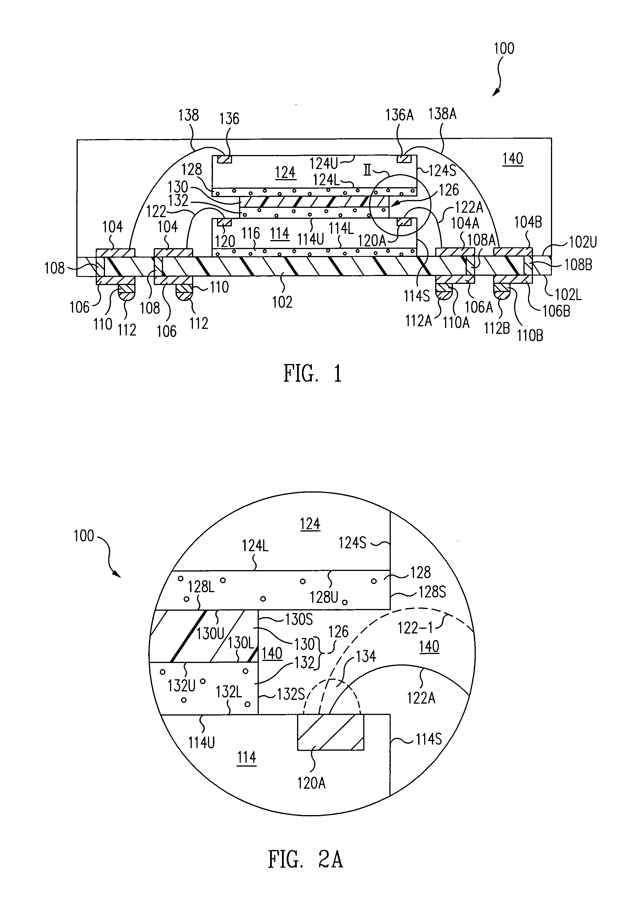
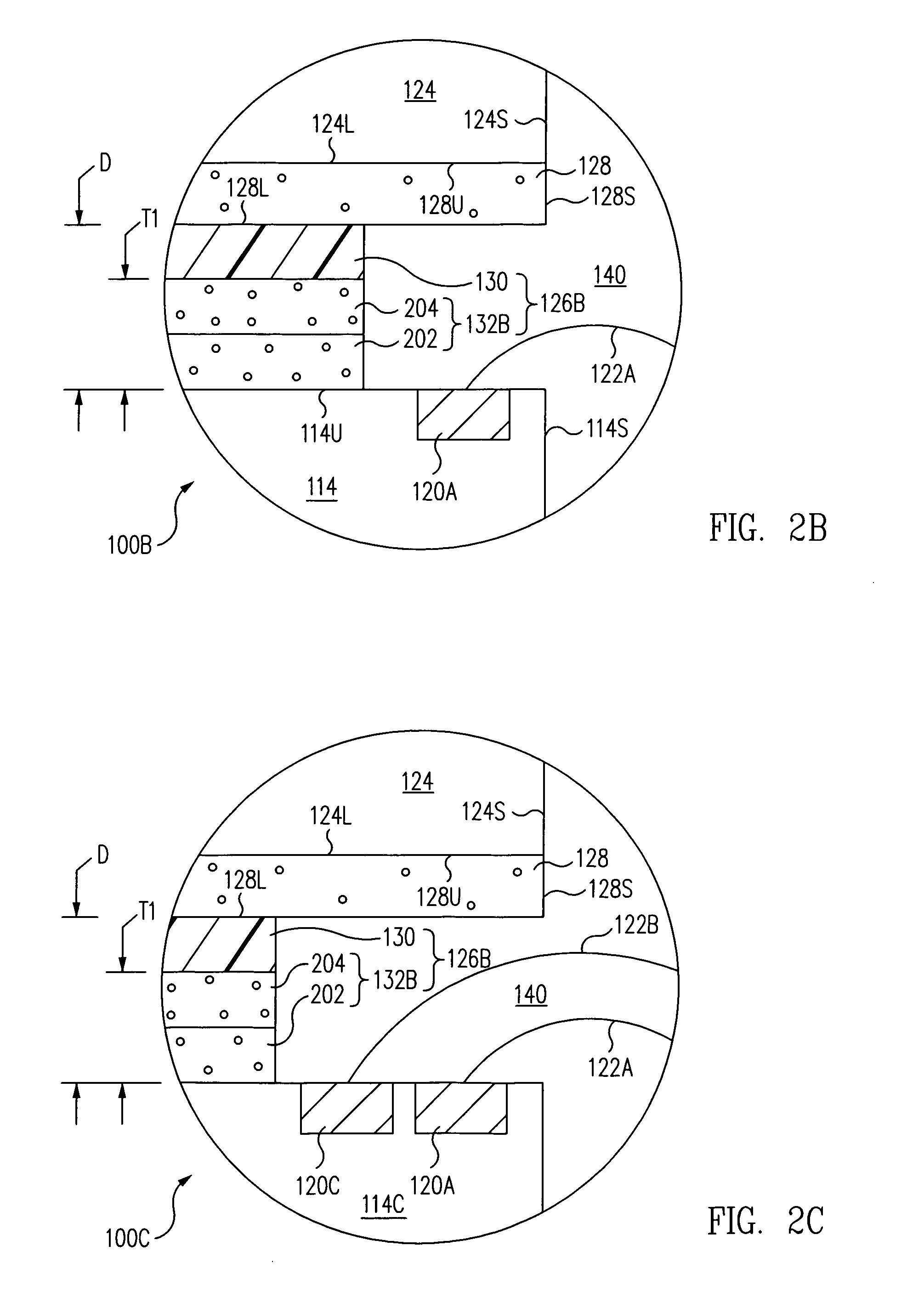
[0021]In accordance with one embodiment, referring to FIG. 4, a method of fabricating a stacked electronic component package 100 includes placing a single-sided film spacer 126 on an upper surface 114U of a lower electronic component 114 inward of bond pads 120 with a pickup tool 404. After being adhered to (pressed on) upper surface 114U of lower electronic component 114, pickup tool 404 is retracted from single-sided film spacer 126.

[0022]An upper surface 130U of a film 130, e.g., an organic film, of single-sided film spacer 126 is not adhesive. Accordingly, single-sided film spacer 126 does not stick to pickup tool 404 during retraction of pickup tool 404 from single-sided film spacer 126. Thus, voiding between single-sided film spacer 126 and lower electronic component 114 and the associated loss of yield of fabrication of stacked electronic component package 100 is minimized. Further, single-sided film spacer 126 is relatively inexpensive compared to a silicon spacer and thus s...


PUM


Abstract

A method of fabricating a stacked electronic component package includes placing a single-sided film spacer on an upper surface of a lower electronic component inward of bond pad with a pickup tool. After being adhered to the upper surface of the lower electronic component, the pickup tool is retracted from the single-sided film spacer. An upper surface of a film, e.g., an organic film, of the single-sided film spacer is nonadhesive. Accordingly, the single-sided film spacer does not stick to the pickup tool during retraction of the pickup tool from the single-sided film spacer.

Description

[0001]This application is related to St. Amand et al., commonly assigned and co-filed U.S. patent application Ser. No. [ATTORNEY DOCKET NUMBER G0090], entitled “STACKED ELECTRONIC COMPONENT PACKAGE HAVING FILM-ON-WIRE SPACER”, which is herein incorporated by reference in its entirety.BACKGROUND OF THE INVENTION[0002]1. Field of the Invention[0003]The present invention relates generally to the packaging of electronic components. More particularly, the present invention relates to a stacked electronic component package and method for fabricating the same.[0004]2. Description of the Related Art[0005]To reduce the size of electronic component packages, electronic components such as semiconductor dies were stacked one upon another within a stacked electronic component package. To space the upper electronic component above the lower bond wires connected to the bond pads of the lower electronic component, a spacer was used.[0006]The spacer was mounted to the upper surface of the lower elec...

Claims


Application Information

Patent Timeline
IPC IPC(8): H01L23/02
CPCH01L23/3128H01L25/0657H01L2224/48091H01L2224/48227H01L2224/73265H01L2224/92247H01L2225/0651H01L2225/06575H01L2924/19103H01L2924/00014H01L24/27H01L2224/32145H01L2224/32225H01L2924/00H01L2924/15311H01L2924/00012H01L2924/181H01L24/73H01L2924/14
Inventor ST. AMAND, ROGER D.HAN, CHANGSUKKIM, YOUNSANGPARK, KYUNGROK
Owner AMKOR TECH INC DW US
Why Eureka
Try Eureka