Circuit board assembly with light emitting element

Inactive Publication Date: 2008-10-09
TYCO ELECTRONICS LOGISTICS AG (CH)
View PDF7 Cites 13 Cited by
  • Summary
  • Abstract
  • Description
  • Claims
  • Application Information

AI Technical Summary

Problems solved by technology

However, as the density of modules and associated components on circuit boards increases, it remains a challenge to accommodate the status

Method used


Image

  • Circuit board assembly with light emitting element
  • Circuit board assembly with light emitting element
  • Circuit board assembly with light emitting element

Examples


Embodiment Construction

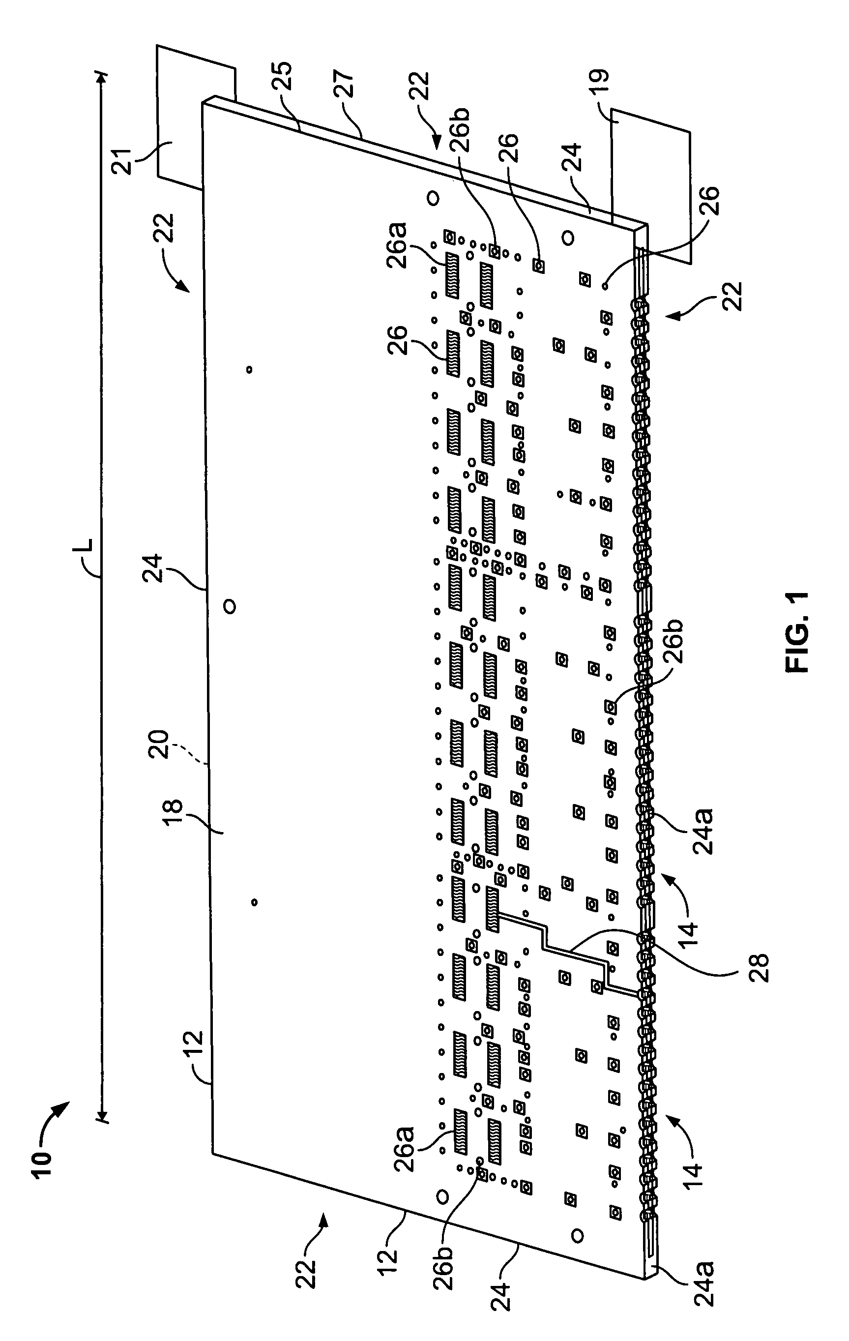
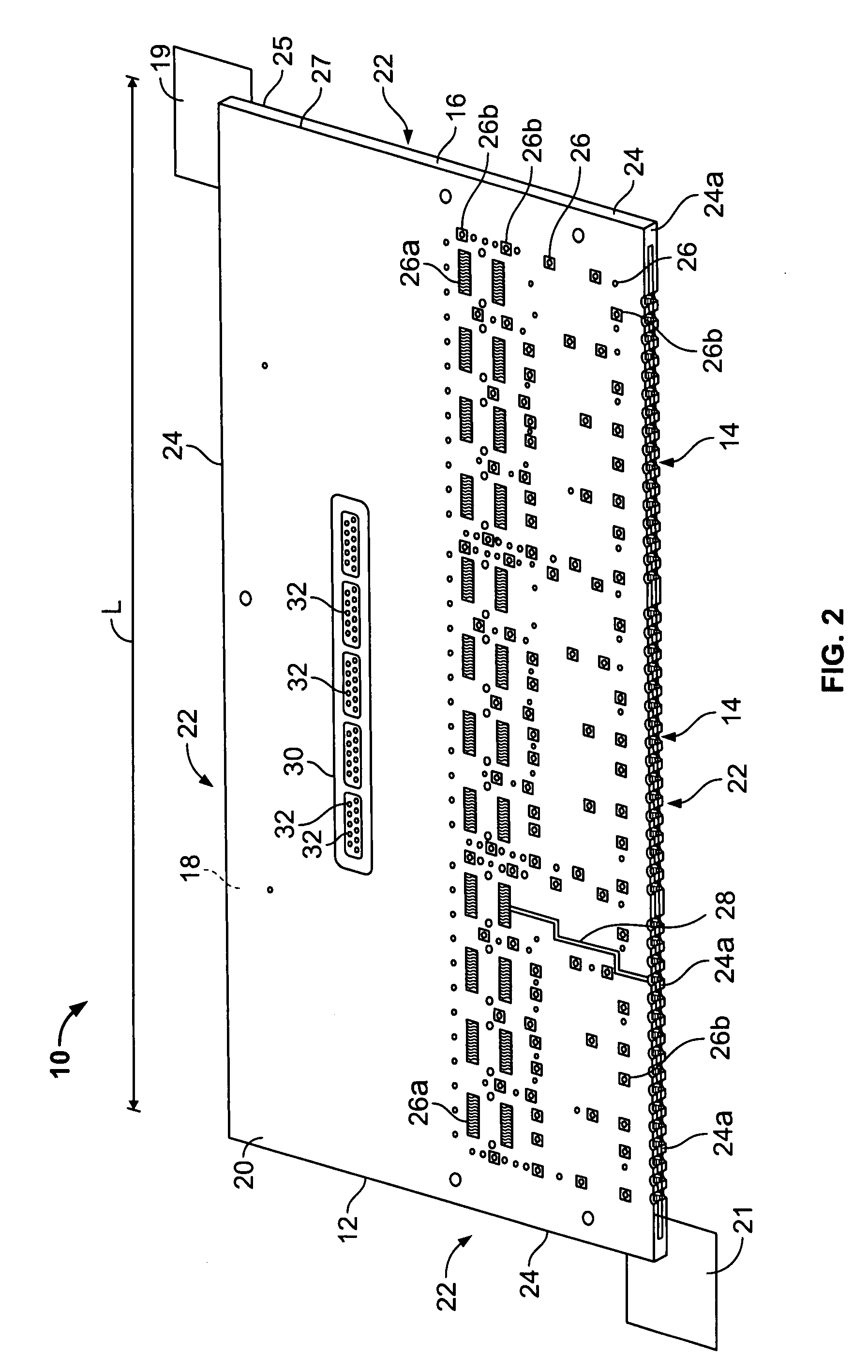
[0017]FIG. 1 is a top perspective view of a circuit board assembly 10 formed in accordance with an exemplary embodiment. FIG. 2 is a bottom perspective view of the circuit board assembly 10. The circuit board assembly 10 includes a circuit board 12 and a plurality of light emitting elements 14 mounted on the circuit board 12. The circuit board 12 includes a dielectric substrate 16 having a pair of opposing surfaces 18 and 20 that each extend between a plurality of edge portions 22. In the exemplary embodiment, the surfaces 18 and 20 are each generally planar and extend substantially parallel to each other. Each of the surfaces 18 and 20 lies within a respective plane 19 and 21. A distance between the planes 19 and 21 defines a thickness T (FIG. 3) of the circuit board 12 adjacent the edge portions 22. Each edge portion 22 includes an edge surface 24 that intersects the surfaces 18 and 20. The intersection between each edge surfaces 24 and the surfaces 18 and 20 defines a respective ...


PUM


Abstract

A circuit board assembly includes a circuit board having opposing first and second surfaces each extending between at least one edge surface that intersects the first and second surfaces. A light emitting element is mounted directly over the edge surface of the circuit board.

Description

BACKGROUND OF THE INVENTION[0001]The invention relates generally to circuit board assemblies, and, more particularly, to circuit board assemblies that include light emitting elements.[0002]Transceiver modules are used for making bi-directional connections to communication devices such as modems, network interfaces, and other electrical components or electrical systems such as computer systems and the like. The Small Form-Factor Pluggable (SFP) standard, which supports both fiber optic and copper based transceivers, includes specifications for transceivers that are reduced in size to achieve a higher port density. Typically, an SFP transceiver module is inserted into a complementary metal cage assembly that is mounted on a circuit board. In order to increase transceiver density on the circuit board, a stacked cage and connector system is sometimes used wherein the transceivers are arranged in rows and columns with each transceiver module plugged into a socket or receptacle in the cag...

Claims


Application Information

Patent Timeline
IPC IPC(8): H05K1/00
CPCH01R13/6658H01R13/7175H05K1/141H05K1/18H05K1/184H05K3/3405H05K3/403H05K7/1461H05K2201/09163H05K2201/09181H05K2201/10106H05K2201/10189H05K2201/10446
Inventor COSTELLO, BRIAN PATRICK
Owner TYCO ELECTRONICS LOGISTICS AG (CH)
Why Eureka
Try Eureka