

Plasma processing apparatus
- Summary
- Abstract
- Description
- Claims
- Application Information
AI Technical Summary
Benefits of technology
Problems solved by technology
Method used
Image

Examples
Embodiment Construction
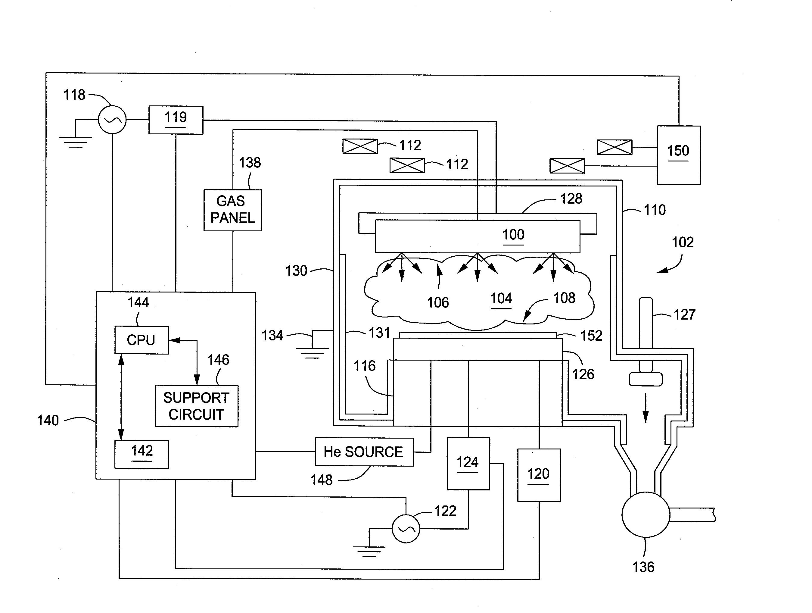
[0017]Embodiments of the present invention generally relate to semiconductor processing apparatus and methods of use thereof. Specifically, embodiments of the present invention relate to a plasma processing apparatus having a plasma control magnet assembly configured to selectively control portions of a plasma and methods of plasma processing therewith.
[0018]The inventive plasma control magnet assembly may be utilized in numerous plasma enhanced processing chambers, such as for example, etch chambers, chemical vapor deposition (CVD) chambers, physical vapor deposition (PVD) chambers, or other chambers configured for plasma processing. One such process chamber suitable for performing the invention is the ENABLER® etch reactor, available from Applied Materials, Inc., of Santa Clara, Calif. This reactor is described in depth in commonly owned U.S. Pat. No. 6,853,141, issued Feb. 8, 2005 to Hoffman, et al., which is herein incorporated by reference in its entirety. As a further non-limi...
PUM
| Property | Measurement | Unit |
|---|---|---|
| Diameter | aaaaa | aaaaa |
| Diameter | aaaaa | aaaaa |
| Magnetic field | aaaaa | aaaaa |
Abstract
Description
Claims
Application Information