
Split wave compensation for open stubs

a split wave compensation and open stub technology, applied in the direction of printed circuit non-printed electric components, high frequency circuit adaptations, instruments, etc., can solve the problems of signal degradation, increased signal layer unavoidable, and increased manufacturing process cos

Active Publication Date: 2008-12-18
FLEXTRONICS AP LLC
View PDF21 Cites 19 Cited by
  • Summary
  • Abstract
  • Description
  • Claims
  • Application Information

AI Technical Summary

Problems solved by technology

Due to the increasing signal density on circuit substrates, an increasing number of signal layers becomes unavoidable.
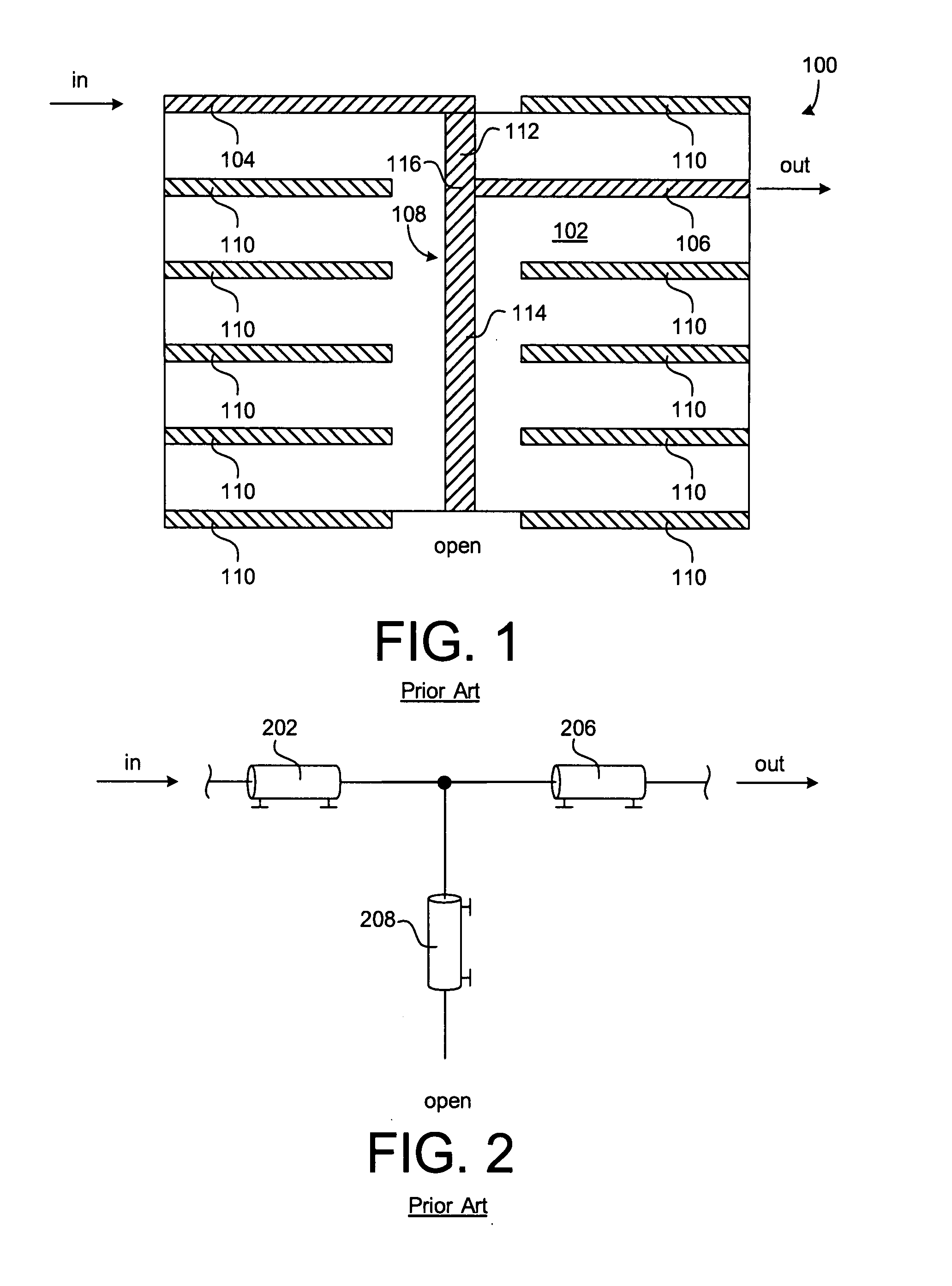
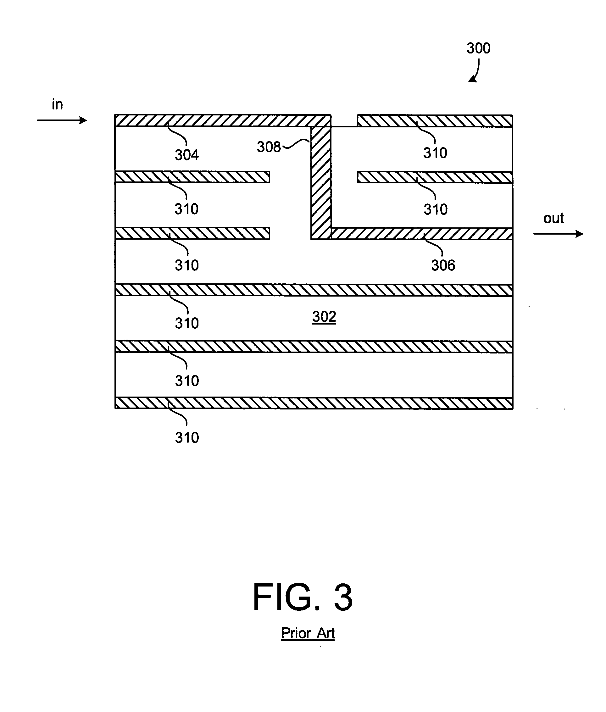
However, at high data-communication speeds, through-hole vias may cause signal degradation.
Although blind vias reduce signal degradation, the manufacturing process adds substantial cost compared to that of typical through-hole vias.
Further, in the case of backplane connectors (through-hole pins), the blind via process is useless.

Method used


Image

  • Split wave compensation for open stubs
  • Split wave compensation for open stubs
  • Split wave compensation for open stubs

Examples


Embodiment Construction

[0026]The following description is provided to enable any person skilled in the art to make and use the invention and is provided in the context of a particular application. Various modifications to the embodiments are possible, and the generic principles defined herein may be applied to these and other embodiments and applications without departing from the spirit and scope of the invention. Thus, the invention is not intended to be limited to the embodiments and applications shown, but is to be accorded the widest scope consistent with the principles, features and teachings disclosed herein.

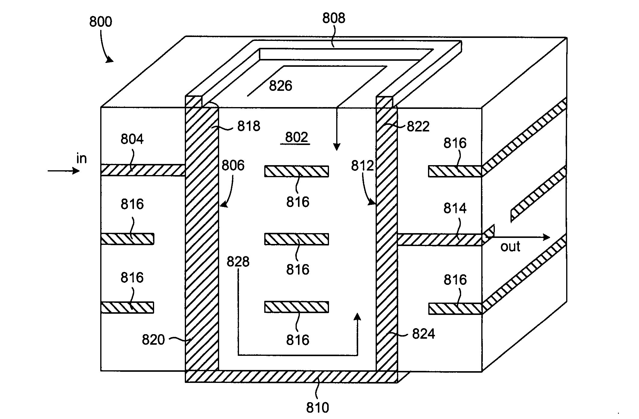
[0027]FIG. 4 shows a cross-sectional perspective view of a multilayer printed circuit board (PCB) 400, in accordance with an embodiment of the present invention. As shown, PCB 400 includes a nonconductive substrate 402, a signal input layer 404, a signal output layer 406, a via 408, a via 410, a first (top) microstrip 412, a second (bottom) microstrip 414, and multiple ground planes 416. One sk...


PUM

PropertyMeasurementUnit
Electrical conductoraaaaaaaaaa
Electric impedanceaaaaaaaaaa

Abstract

In accordance with a first embodiment, the present invention provides a circuit substrate comprising a first surface; a second surface; a first via having a first end near said first surface and a second end near said second surface; a second via having a first end near said first surface and a second end near said second surface; a first conductive element electrically coupling said first end of said first via and said first end of said second via; a second conductive element electrically coupling said second end of said first via and said second end of said second via; an input signal line coupled to said first via; and an output signal line coupled to said second via.

Description

BACKGROUND[0001]1. Technical Field[0002]This invention relates generally to multilayer circuit substrates, and more particularly to conductive vias that facilitate signal propagation between intermediate layers within circuit substrates.[0003]2. Description of the Background Art[0004]A typical circuit substrate includes multiple conductive layers separated by electrically insulated layers. Such conductive layers intercommunicate using vias formed in the circuit substrate. Generally, vias are perpendicular bores formed through the layers of a circuit substrate by processes such as laser drilling. Such bores are filled or lined with conductive material as needed to provide electrical communication paths between the conductive layers. Vias typically pass through the entire circuit substrate, even if for example the top layer is communicating with a middle layer. Such vias are commonly known as “through-hole vias.”[0005]As data-communication speeds increase, signal integrity becomes cru...

Claims


Application Information

Patent Timeline
IPC IPC(8): H01R12/04H05K3/02
CPCH05K1/0248H05K1/0251H05K3/429H05K2201/09336Y10T29/49165H05K2201/0979Y10T29/49155Y10T428/24917H05K2201/09627Y10T428/31511
Inventor GORCEA, DAN
Owner FLEXTRONICS AP LLC
Learn More