Resistance change memory device

a memory device and resistance change technology, applied in the direction of information storage, static storage, digital storage, etc., can solve the problem of not being able to propose a detailed configuration of a cell array and a read/write circui

Inactive Publication Date: 2008-12-18
TOSHIBA MEMORY CORP
View PDF16 Cites 40 Cited by
  • Summary
  • Abstract
  • Description
  • Claims
  • Application Information

AI Technical Summary

Benefits of technology

[0012]the variable resistance element includes a recording layer formed of a first composite compound expressed by AxMyOz (where “A” and “M” are cation elements different from eac

Problems solved by technology

However, there has not been proposed a detailed configuration of a cell array and a read/write circuit thereof.
In order to achieve a practical non-volatile memory with a high density and a high performance, how to combine

Method used


Image

  • Resistance change memory device
  • Resistance change memory device
  • Resistance change memory device

Examples


Embodiment Construction

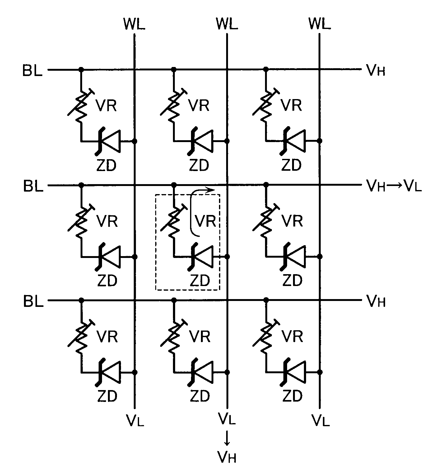
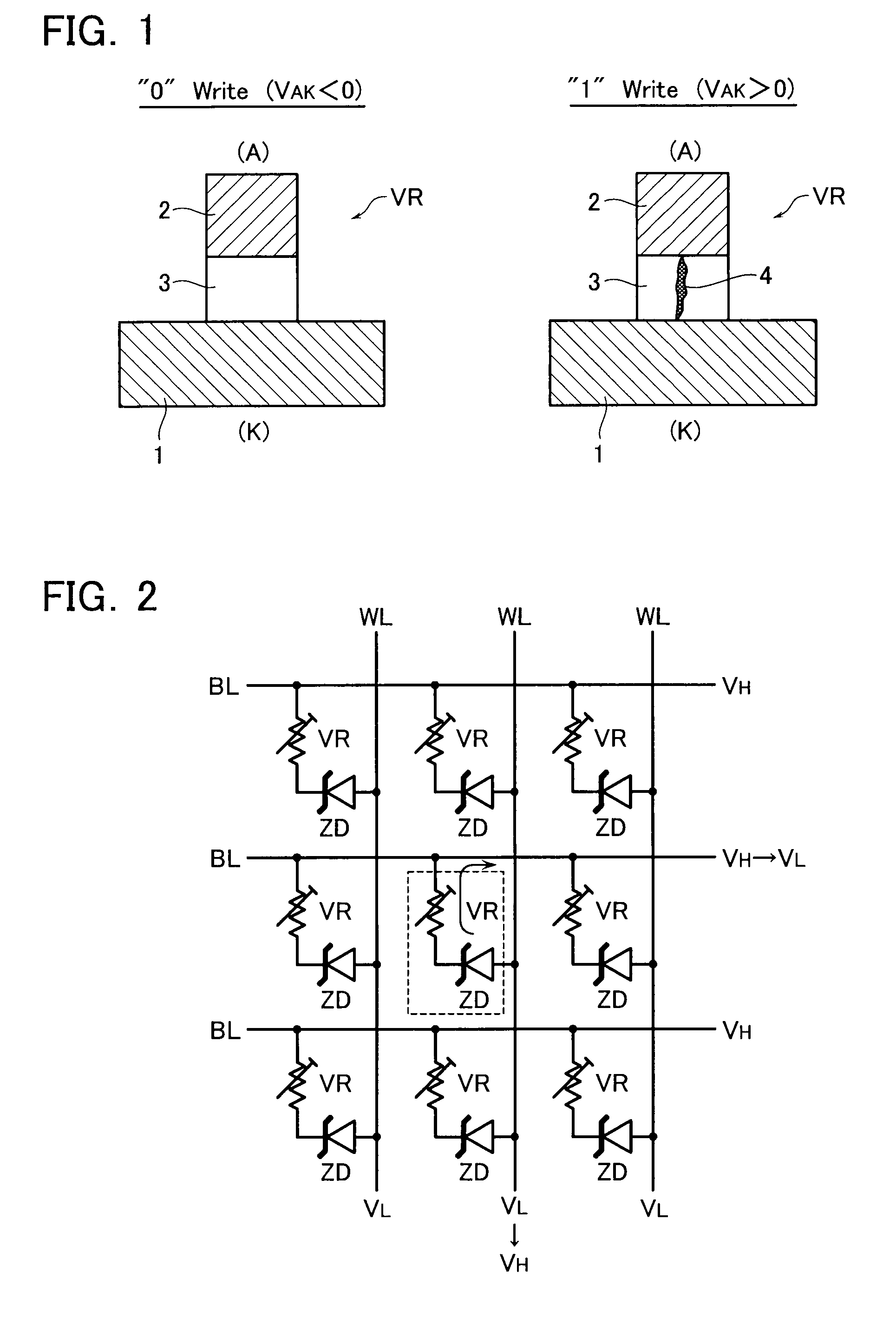
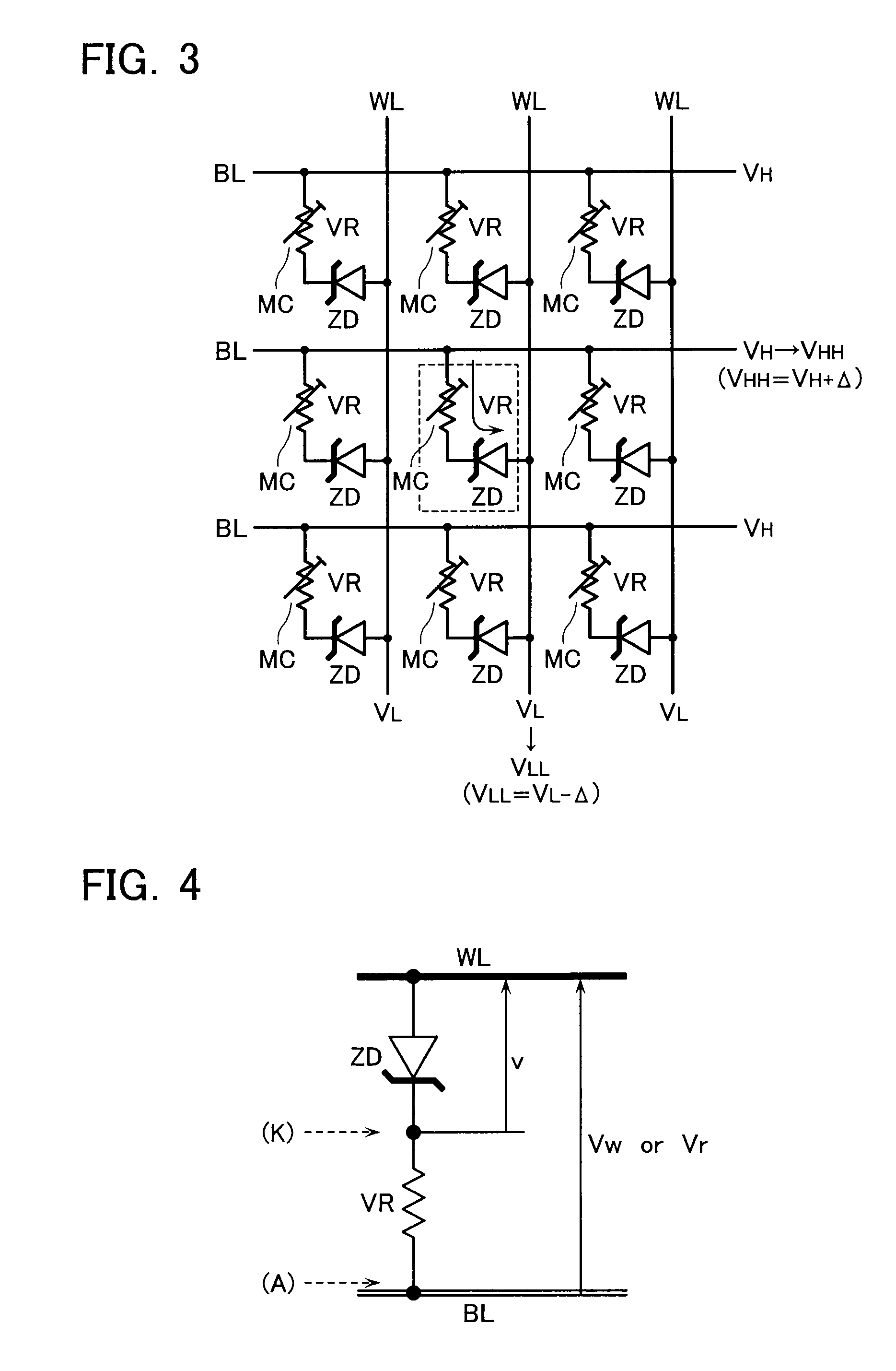
[0046]FIG. 1 shows a principle configuration of a programmable resistance (variable resistance) VR used in the present invention. The programmable resistance VR is formed of a resistance film 3 as being a memory material, and cathode, anode electrodes 1, 2 that sandwiches the resistance film 3.

[0047]The resistance film 3 is, for example, an ion conductor (solid electrolyte) formed of a chalcogenide containing metal ions such as silver, cupper and the like. For example, Ge—S, Ge—Se and the like may be used as the chalcogenide. When the resistance film 3 is formed of the above-described chalcogenide, the electrodes 1, 2 are also formed containing silver therein.

[0048]The resistance film 3 stores, for example, a high resistance state as a data “0” and a low resistance state as a data “1”. In this programmable resistance VR, apply a positive anode-cathode voltage (VAK>0) that is over a threshold value, and a data “1” will be written. Apply a negative anode-cathode voltage (VAKAK>0, a co...


PUM


Abstract

A resistance change memory device including: a semiconductor substrate; at least one cell array formed above the semiconductor substrate, each memory cell having a stack structure of a variable resistance element and an access element, the access element having such an off-state resistance value in a certain voltage range that is ten times or more as high as that in a select state; and a read/write circuit formed on the semiconductor substrate as underlying the cell array, wherein the variable resistance element comprises a recording layer formed of a first composite compound expressed by AxMyOz (where “A” and “M” are cation elements different from each other; “O” oxygen; and 0.5≦x≦1.5, 0.5≦y≦2.5 and 1.5≦z≦4.5) and a second composite compound containing at least one transition element and a cavity site for housing a cation ion.

Description

CROSS REFERENCE TO RELATED APPLICATION[0001]This is a continuation of U.S. application Ser. No. 11 / 761,397, filed on Jun. 12, 2007. U.S. application Ser. No. 11 / 761,397 is incorporated herein by reference.BACKGROUND OF THE INVENTION[0002]1. Field of the Invention[0003]This invention relates to a resistance change memory device, which stores a resistance value determinable by a resistance change of memory material in a non-volatile manner.[0004]2. Description of the Related Art[0005]Recently, there have been proposed some memory devices having variable resistance elements. One of such the memory devices is known as a phase change memory which uses phase transition between an amorphous state and a crystalline state of a memory material (for example, U.S. Pat. No. 6,314,014B1). In such the phase change memory device, by controlling the current of a chalcogenide cell, reversible switching may be performed between a crystalline state (i.e. low resistance state) and an amorphous state (i....

Claims


Application Information

Patent Timeline
IPC IPC(8): G11C11/00
CPCG11C13/0004G11C13/0007G11C13/0011G11C13/0014G11C13/0016G11C13/004G11C2013/0042G11C2213/31G11C2213/32G11C2213/55G11C2213/56G11C2213/71G11C2213/72
Inventor TODA, HARUKIKUBO, KOICHI
Owner TOSHIBA MEMORY CORP
Why Eureka
Try Eureka