

Light sensor located above an integrated circuit
a technology of integrated circuits and light sensors, applied in the field of microelectronics, can solve the problems of low performance, low efficiency, and loss of parts of the structure, and achieve the effect of minimising dark current and optimal electric qualities
- Summary
- Abstract
- Description
- Claims
- Application Information
AI Technical Summary
Benefits of technology
Problems solved by technology
Method used
Image

Examples
Embodiment Construction
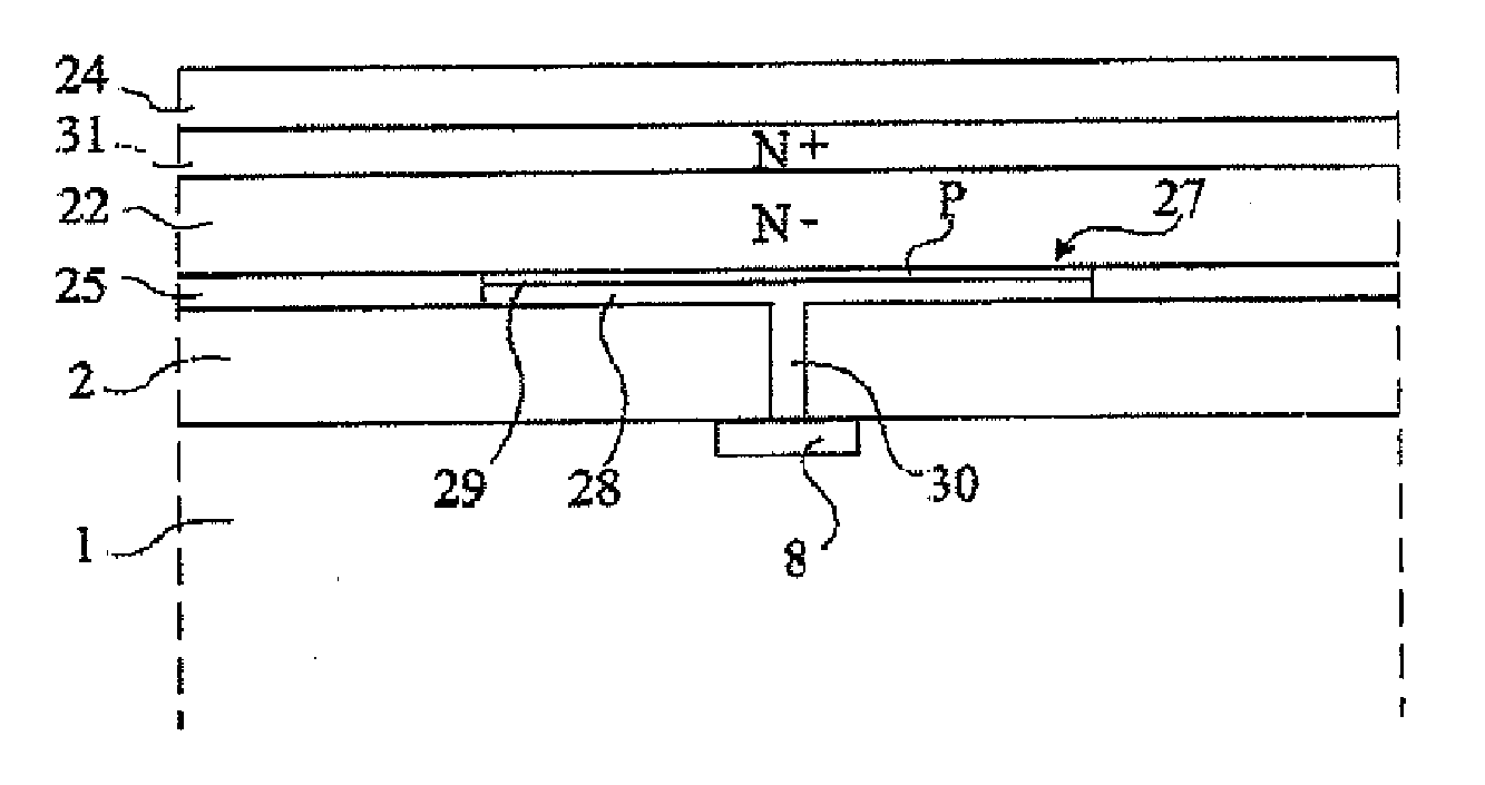
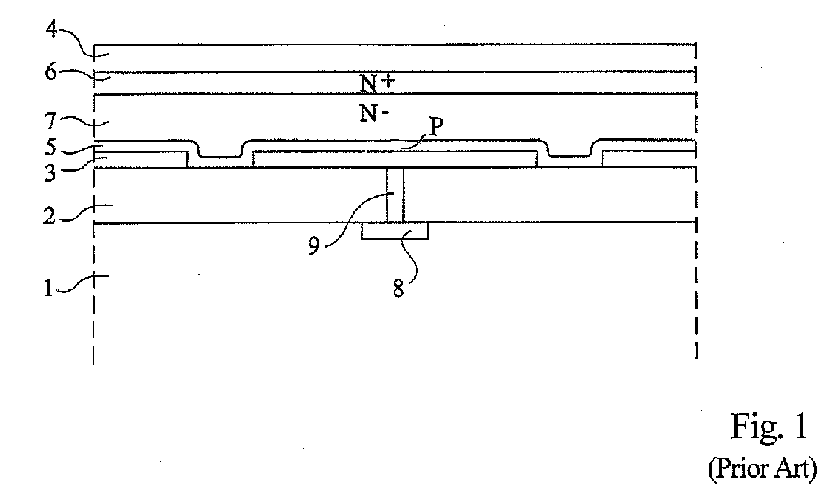
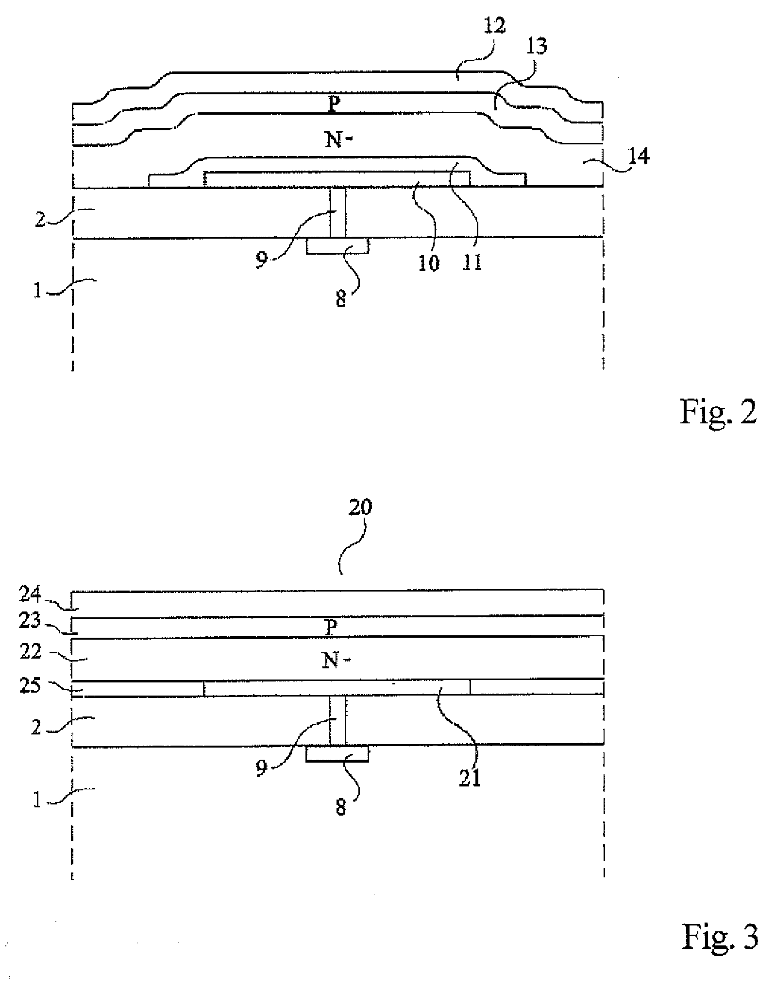
[0029]As usual in the representation of integrated circuits, the scales are not respected in the different cross-section views to better show the different layers and elements of the devices.
[0030]In an attempt to simplify the prior art structure illustrated in FIG. 1, the applicant has formed the structures shown in FIG. 2. FIG. 2 describes an integrated circuit formed in a substrate 1. An insulating layer 2, comprising metal interconnects, is formed above the circuit. Above insulating layer 2 are formed the light-emitting diodes. The light-emitting diodes comprise a lower electrode 10 formed of a titanium nitride layer (TiN) entirely covered with a chromium layer 11 and an upper indium and tin oxide (ITO) electrode 12. The upper electrode is in electric contact with an underlying P-type doped amorphous silicon 13. Between electrode 11 and the P-doped amorphous silicon layer, a lightly-doped N-type amorphous silicon layer 14 has been formed. Thus, the structure of FIG. 2 likely to ...
PUM
 Abstract
Description
Claims
Application Information