Manufacturing method of thin film transistor and manufacturing method of array substrate

A technology of thin film transistors and manufacturing methods, applied in the field of liquid crystal display manufacturing

Active Publication Date: 2018-05-11
WUHAN CHINA STAR OPTOELECTRONICS SEMICON DISPLAY TECH CO LTD
View PDF4 Cites 3 Cited by
  • Summary
  • Abstract
  • Description
  • Claims
  • Application Information

AI Technical Summary

Problems solved by technology

[0006] In order to solve the problems existing in the above-mentioned prior art, the present invention provides a method for manufacturing a thin film transistor, which can avoid the use of copper stripping solution when etching the back channel, and instead use a c

Method used


Image

  • Manufacturing method of thin film transistor and manufacturing method of array substrate
  • Manufacturing method of thin film transistor and manufacturing method of array substrate
  • Manufacturing method of thin film transistor and manufacturing method of array substrate

Examples


Embodiment 1

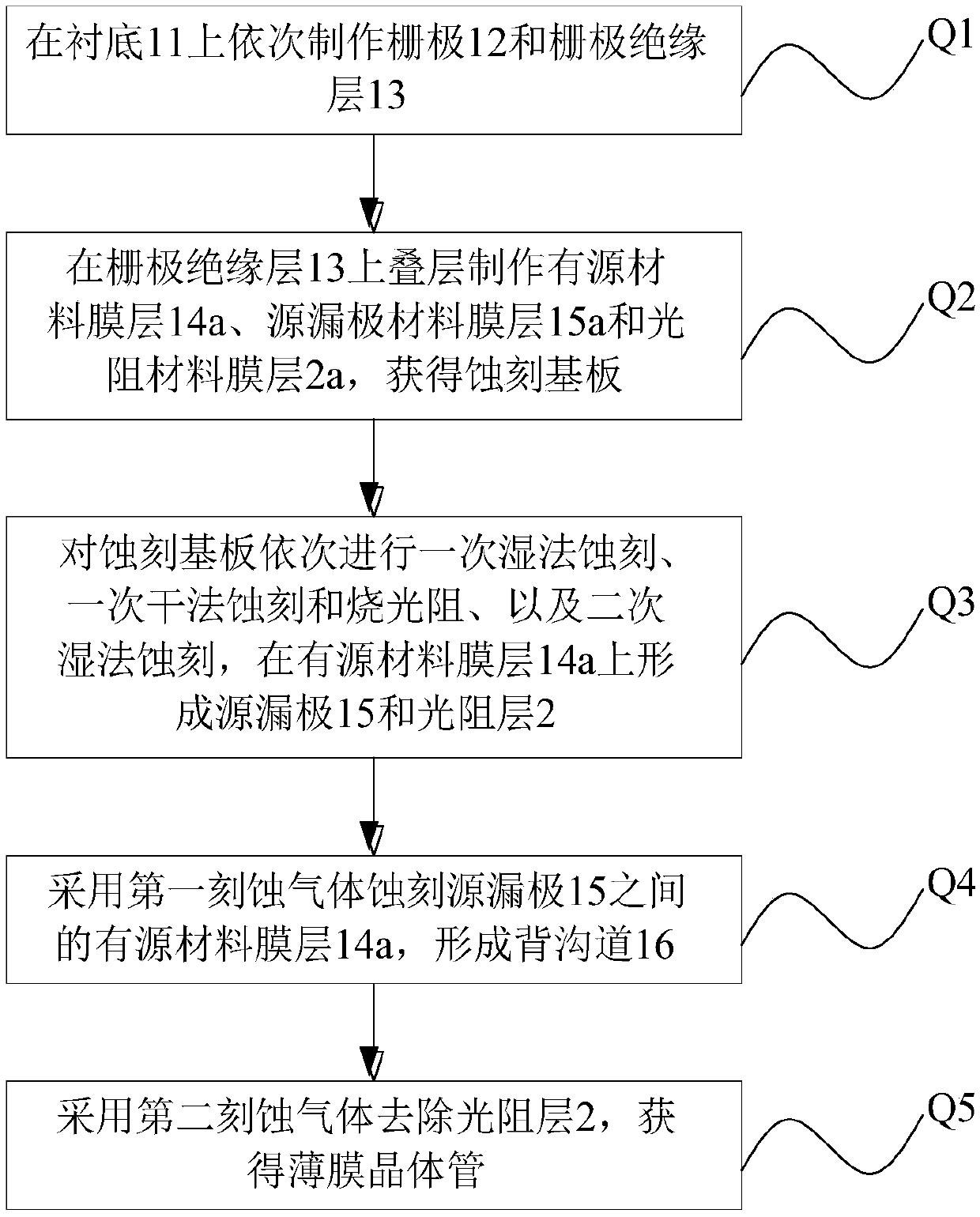
[0027] figure 1 It is a flow chart of the steps of the manufacturing method of the thin film transistor according to the embodiment of the present invention.

[0028] specific reference figure 1 , the manufacturing method of the thin film transistor according to the present embodiment includes the following steps:

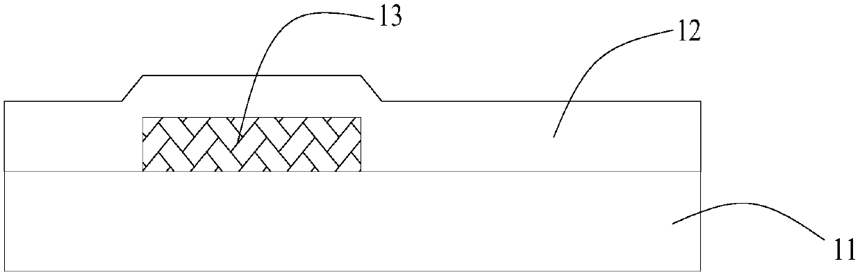
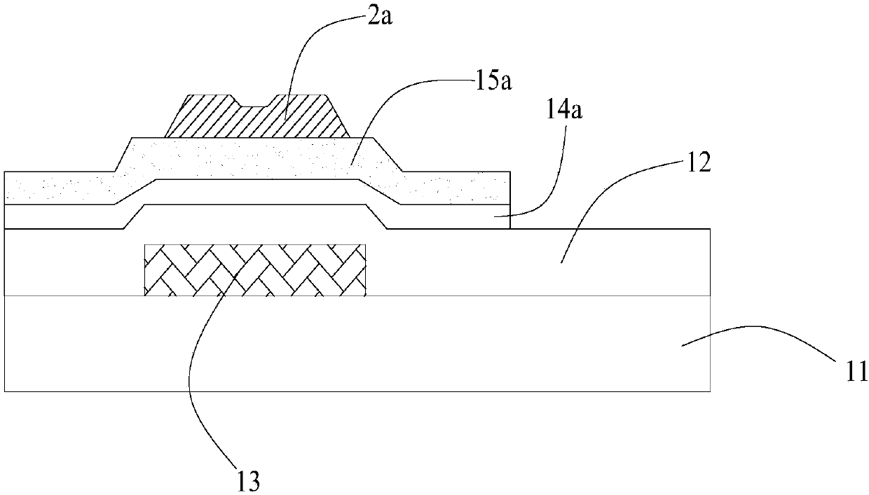
[0029] Step Q1, sequentially fabricating the gate 12 and the gate insulating layer 13 on the substrate 11; figure 2 shown.

[0030] The selection of the substrate 11 and the material selection and process for making the gate 12 and the gate insulating layer 13 thereon will not be repeated here, and those skilled in the art can refer to the prior art; for example, the substrate 11 can be made of glass lining Bottom, etc., the material of gate 12 can be Mo / Cu laminated material or Ti / Mo / Cu laminated material, and the material of gate insulating layer 13 can be SiN x ; Preferably, if the material of the gate 12 is a Mo / Cu laminated material, the thickness of the ...

Embodiment 2

[0048] This embodiment provides a method for fabricating an array substrate, which includes fabricating thin film transistors and elements such as pixel electrodes connected to the thin film transistors; The manufacturing methods of other components can refer to the existing technology, and will not be repeated here. For example, an insulating protective layer is first formed on the thin film transistor, and then holes are opened on the insulating protective layer to form a via structure, and then through physical sputtering Precipitate a layer of ITO and other transparent conductive materials to form pixel electrodes and the like.


PUM


Abstract

The invention provides a manufacturing method of a thin film transistor. A method for forming a back channel comprises the following steps: S21, laminating and manufacturing an active material film, asource and drain electrode material film and a photoresist material film on a gate insulation layer so as to obtain an etched substrate; S22, carrying out primary wet etching, primary dry etching andphotoresist burning and secondary wet etching on the etched substrate in sequence so as to form a source electrode, a drain electrode and a photoresist layer; S23, etching the active material film byadopting a first etching gas so as to form the back channel; and S24, removing the photoresist layer by adopting a second etching gas so as to obtain the thin film transistor. According to the manufacturing method, a copper stripping solution can be avoided from being used when the back channel is etched, and the compositions and using amounts of various etching gases are reasonably matched, so that the problems of copper ion diffusion and pollution of other impurity ions in the copper stripping solution in the prior art are further avoided while back channel etching and photoresist removal are completed. The invention also provides application of the manufacturing method in an array substrate.

Description

technical field [0001] The invention belongs to the technical field of liquid crystal display manufacturing, and specifically relates to a method for manufacturing a thin film transistor and a method for manufacturing an array substrate based on the method for manufacturing the thin film transistor. Background technique [0002] With the continuous development of display technology, thin film transistor liquid crystal display (Thin Film Transistor Liquid Crystal Display, TFT-LCD) occupies a dominant position in the field of flat panel display due to its advantages of small size, low power consumption, and no radiation. As people's pursuit of display resolution and picture refresh rate is getting higher and higher, the development of new materials and new processes is imminent. [0003] At present, the traditional conductive layer metal materials are mainly aluminum and molybdenum. The advantages of aluminum and molybdenum are that the film forming process is simple, the adhe...

Claims


Application Information

Patent Timeline
IPC IPC(8): H01L21/77H01L21/306H01L27/12
CPCH01L21/30604H01L27/1259H01L27/127
Inventor 孙涛
Owner WUHAN CHINA STAR OPTOELECTRONICS SEMICON DISPLAY TECH CO LTD
Why Eureka
Try Eureka