[0004]With an ongoing
miniaturization of
IC devices, especially with
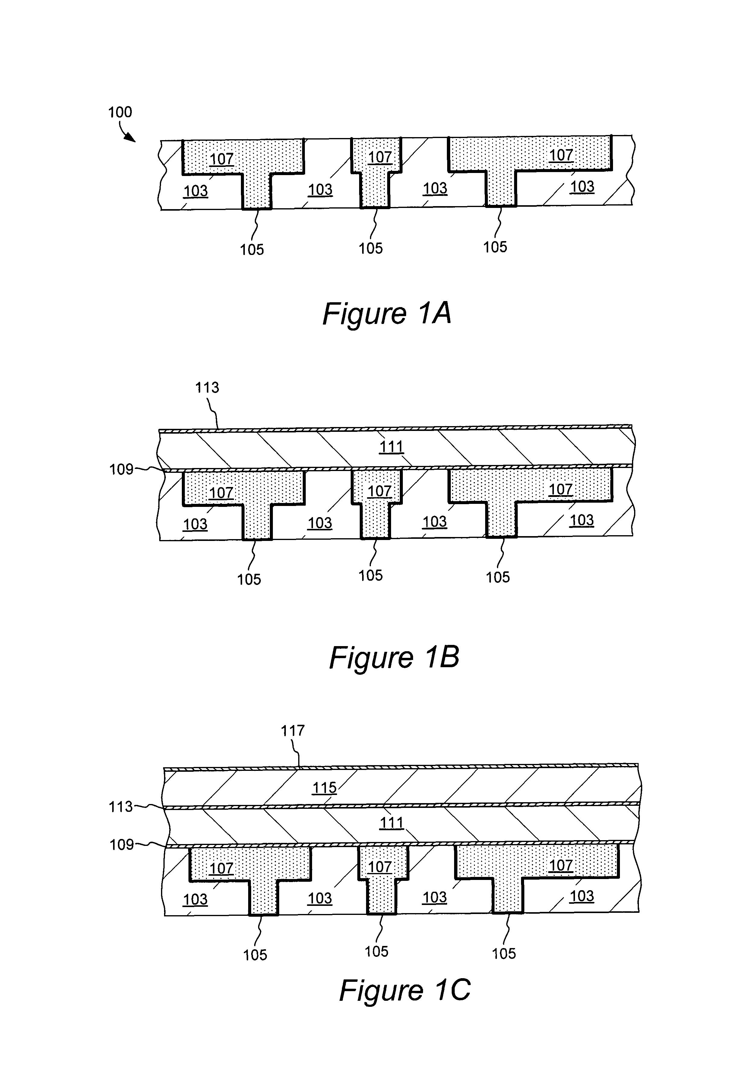
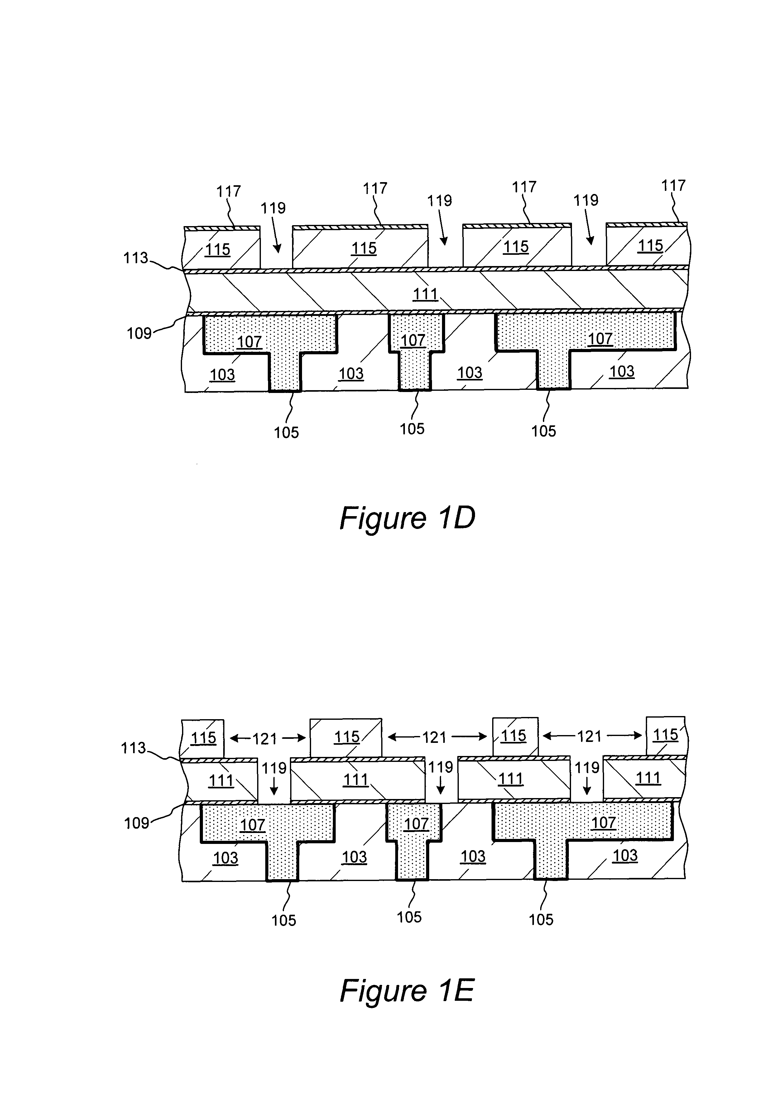
processing of devices at a 65 nm technology node and at more advanced nodes, it became more challenging to perform resputtering without exposing dielectric layers to plasma. It was noted that a layer of dielectric can become exposed during resputter, especially when large amounts of
diffusion barrier or other material are removed from the wafer substrate. When resputtering is performed under conventional conditions, the exposed dielectric material can easily become damaged by high-energy ions that impinge upon it. One type of such damage is microtrenching, which manifests itself in increased dielectric etching at particular locations within the recessed features of the wafer. In one typical example, microtrenches are formed in the proximity of the sidewalls in the bottom portions of the recessed features, e.g., in the trench bottoms. Microtrenching leads to decreased reliability of the formed IC devices due to reduced adhesion of the subsequently deposited layers. Further, microtrenching contributes to an increase in line-to-line leakage due to local increase in current densities in the microtrenches. It was therefore recognized that there is a need for a resputtering method that would remove material from the wafer surface without causing microrotrenching in the exposed
dielectric layer.
[0005]Efficient resputtering of
diffusion barrier layers in the presence of exposed dielectric can be achieved when higher density plasma is employed. Microtrenching can be substantially eliminated when resputtering is performed using a
high flux of low energy ions at the wafer surface. For example, an ion flux of at least about 5·1015 ions / cm2s, preferably of at least about 1016 ions / cm2s, having a mean energy of less than about 250 eV, preferably less than about 200 eV, e.g., less than about 150 eV is effective for
diffusion barrier material etching without causing microtrenching in many types of low-k dielectrics. It is understood that different types of dielectric materials may have different susceptibility to plasma damage, and that lower energy plasma may be needed to avoid microtrenching in more delicate dielectrics, while higher energy plasma may be tolerated by more robust dielectric materials. Without being bound by a particular theory of operation, it is believed that lower
kinetic energy of the ions contacting the wafer leads to decreased dielectric damage, while the higher density of ion flux increases the etch rate and maximizes resputtering efficiency.
[0006]High ion flux of low-energy ions can be produced in one embodiment by generating a high-density low
ion energy plasma
proximate the wafer substrate. Conventionally, generation of plasma having a density of greater than about 1011 electrons / cm3 proximate the wafer substrate, proved to be difficult to achieve. Therefore, high ion fluxes needed for resputtering in low energy regime, could not be easily attained. Further, as higher density plasmas were generated, the radial uniformity of an ion flux across the wafer diminished, resulting in higher rates of
material removal at the center of the wafer compared to wafer edges. It was recognized that new methods and apparatus for increasing local
plasma density and for improving plasma uniformity were needed.
[0007]According to some embodiments presented herein,
plasma density of at least about 5·1011 electrons / cm3 (or ions / cm3), preferably at least about 1012 electrons / cm3 and, in some cases, as high as at least about 1013 electrons / cm3 is achieved in the vicinity of the wafer surface (e.g., within about 3 cm of the wafer surface, such as within 1 cm of the wafer surface). Increased ion flux provided by such plasma achieves efficient etching of
diffusion barrier or other material, even when the
kinetic energy of ions in the plasma is relatively low.
[0009]While methods and apparatus described herein address the microtrenching problem by providing
high density low energy plasmas at the wafer surface, the described methods and apparatus are not limited to this particular application. In general, these methods can be used for increasing local plasma density in a variety of processes, including both resputtering (in a low energy and
high energy regimes) and deposition. While provided methods are particularly suitable for resputtering in a low-energy regime, in those instances when dielectric is not exposed during resputtering, higher energy plasmas may be used to increase the etching rates. In yet other embodiments provided methods may be used for depositing
diffusion barrier and seed layer materials. When
high density low
ion energy plasmas are used during deposition, the quality of deposited films can improve, due to decreased incorporation of
inert gas ions into deposited films. In yet other embodiments provided methods are used to generate plasmas, that do not necessarily have
high density, but have higher density than they would otherwise have in a conventional apparatus.
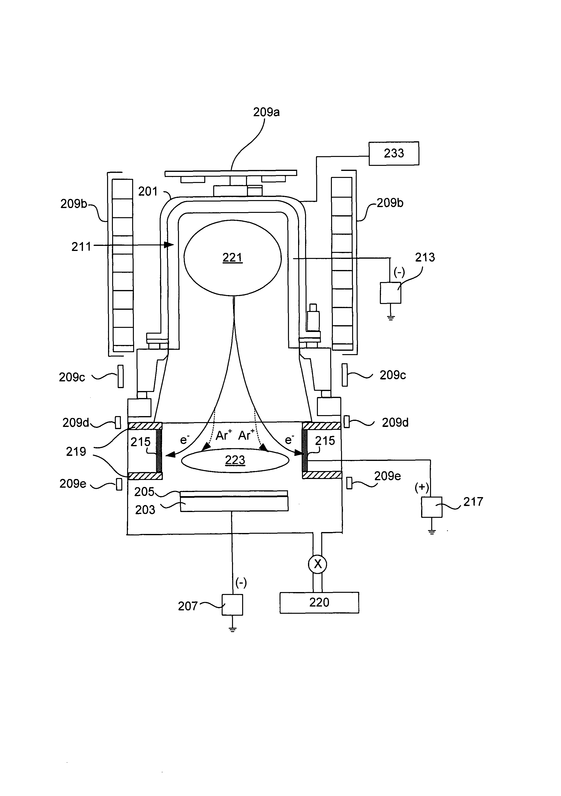
[0018]In those embodiments, where the plasma in the second plasma region is further magnetically confined, it is often preferable to increase plasma density in the second plasma region using a combination of electric and magnetic fields. In one embodiment the E vector (characterizing the
electric field generated by the positively biased ion extractor) and the B vector (characterizing the
magnetic field in the second
plasma confinement region) are substantially orthogonal at least at one location. The generated electromagnetic forces further accelerate the trapped electrons in this region and produce a region of higher density plasma. In one implementation, the formed plasma is toroidally shaped above the wafer, and contributes to non-uniformity improvement at the wafer edges.

